No part of this document may be reproduced, transmitted, photocopied, or translated into another language without the written consent of EPIX, Inc. Information in this document is subject to change without obligation or notice. EPIX, Inc. makes no warranty of any kind with regard to this document, including, but not limited to, the implied warranties of merchantability and fitness for a particular purpose. EPIX, Inc. assumes no responsibility for any errors that may appear in this document. EPIX, Inc. reserves the right to make changes to the specifications of hardware and software at any time, without obligation or notice.
4MIP, SVIP, XCIP, XCAP, 4MEG VIDEO, 1MEG VIDEO, SILICON VIDEO MUX, QUICK SET VIDEO, 12-7MUX, IMAGE MEMORY EXPANSION, COC40, and COC402 are trademarks of EPIX, Inc.
EPIX, SILICON VIDEO, and PIXCI are registered trademarks of EPIX, Inc.
Other brand, product, and company names are trademarks or registered trademarks of their respective owners.
Printing: 11-Feb-2023
EPIX, Inc.
381 Lexington Drive
Buffalo Grove IL 60089
847.465.1818
847.465.1919 (fax)
epix@epixinc.com
www.epixinc.com
Table of Contents
- 1. Installation
- 2. Connectors
- 3. Software
Installation
- 3.1. For Windows 8/10/11/ 32/64-Bit
- 3.2. Windows 8/10/11 32/64-Bit Esoterica
- 3.3. For Windows 7 32/64-Bit
- 3.4. Windows 7 32/64-Bit Esoterica
- 3.5. For older versions of Windows
- 3.6. For Linux
- 3.7. Linux Esoterica
- 3.8. For older versions of Linux
- 3.9. PIXCI® Driver Esoterica
- 4. Getting
Started with XCAP
- 4.1. Start XCAP
- 4.2. Open PIXCI® Frame Grabber
- 4.3. PIXCI® D, D24, D32, D2X, D3X Video Configuration
- 4.4. Capturing Images
- 4.5. Examining Images
- 4.6. PIXCI® D, D24, D32, D2X, D3X Video Adjustments
- 4.7. Saving Images
- 4.8. Capturing an Image Sequence
- 4.9. Saving Image Sequences
- 4.10. Additional XCAP Documentation
- 5. XCAP Software
Guide
- 5.1. The Main Window
- 5.2. The
Image Viewer Window
- 5.2.1. Image Viewer - File
- 5.2.2. Image Viewer - View
- 5.2.3. Image Viewer - Examine
- 5.2.4. Image Viewer - Modify
- 5.2.5. Image Viewer - Measure
- 5.2.6. Image Viewer - Draw
- 5.2.7. Image Viewer - AOI
- 5.2.8. Image Viewer - View - Shortcuts
- 5.2.9. Image Viewer - View - Status Bar
- 5.2.10. PIXCI® Image Viewer - Capture
- 5.2.11. PIXCI® Image Viewer - Capture - Shortcuts
- 5.3. Other Features
- 5.4. Road Map - Main Window
- 5.5. Road Map - PIXCI® Image Viewer Window
- 5.6. XCAP Software Feature Comparison
- 6. Getting
Started with XCLIB
- 6.1. XCLIB Architecture Overview
- 6.2. The Simplest XCLIB Program
- 6.3. XCLIB Error Detection
- 6.4. PIXCI® D, D24, D32, D2X, D3X Video Configuration
- 6.5. More Video Capture Modes
- 6.6. PIXCI® D, D24, D32, D2X, D3X Triggered Capture
- 6.7. PIXCI® D, D24, D32, D2X, D3X Triggered Sequence Capture
- 6.8. Additional XCLIB Documentation
- 7. Specifications
- 8. Camera Control Registers
- 9. In Case of Trouble
- 10. Hardware Revision Description
- 11. Certification and Warranty
- 12. Footnotes
1. Installation
Thank you for purchasing imaging products from EPIX, Inc. We are available via the Internet, FAX, and telephone to help with installation or to answer questions about the use of our products for your application.
The PIXCI® D3X frame grabber, for the PCI bus, is packed in a static dissipative bag. Prior to opening the bag, place the bag near the PC into which the frame grabber will be installed.
1.1. Instructions
We recommend installing XCAP prior to installing the PIXCI frame grabber. Please refer to the Software Installation chapter for the XCAP installation directions, then follow the frame grabber installation instructions below.- Turn off the power and remove the cover from the PC into which the PIXCI frame grabber is to be installed.
- Select a vacant PCI bus slot and remove the metal bracket and screw covering the back panel slot with which it is aligned. Consult the reference manual for the PC if there is any doubt about which slot is a PCI bus slot.
- Use of a static free area and a wrist strap connected to the PC or to the static free area is suggested during installation. Walking can generate static electricity. Keep your feet stationary while removing the PIXCI frame grabber from the anti-static bag. Hold the bag and the PC at the same time, or place the bag on the PC chassis and hold the chassis to dissipate the static charge that may have been created while transporting the frame grabber to the PC.
- Remove the PIXCI frame grabber from the anti-static bag and insert it into the PCI bus connector. This can require up to 15 pounds of force. Do not use too much force as the frame grabber may not be inserted into the connector correctly, and the result can be damage to the connector and the frame grabber. Consult the reference manual for the PC if there is any doubt about which slot is a PCI bus slot. Note that some computers have 3.3 volt PCI bus slots or may have 64 bit, 66 MHz PCI slots. The PIXCI D3X frame grabber may be installed in 3.3 volt and 66 MHz PCI slots. When the PIXCI D3X frame grabber is installed in a 66 MHz slot, other cards installed in 66 MHz slots will not be operate faster than 33 MHz.
- Replace the screw to secure the PIXCI frame grabber in the slot.
- Remove the power from all equipment to be connected.
- Connect the cable(s) between the PIXCI, camera, and power supply. The PIXCI end of the cable has a 68 or 100 pin SCSI style subminiature D connector. Do not plug it into a SCSI card. Connect the other end of the cable into the labelled camera connectors.
- Power up the camera, PC, and monitor(s).
- Operate XCAP by following the instructions in the Software Installation and Getting Started chapters in this manual.
- Check for display of video on the VGA monitor by clicking on the Capture and then the Snap menu in the View window or by using the shortcut menu.
- Note that for line scan cameras, either an external vertical drive signal or the ''Internal'' vertical drive selection must be used.
- If there is no video displayed, check for the presence of vertical drive by clicking on ''PIXCI,'' ''PIXCI Status,'' and ''PIXCI-Unit x Status'' (where x is the number of the frame grabber being used). The number reported in the ''Vertical Sync Count'' box should be increasing if vertical drive is being received from the camera. If it is not increasing, check the connections and power to the camera. If that fails, refer to the ''In Case of Trouble'' chapter in this manual.
1.2. Computer
The size and the number of images that can be stored in DRAM on the motherboard is a function of the amount of DRAM that can be spared by the operating system. XCAP, by default, reserves 16 MB of memory for image buffers. If more memory is required for image sequences, the ''Driver Assistant'' (via the menubar's PIXCI®, PIXCI® Open/Close) can be used to request additional frame buffer memory.The PIXCI frame grabber can capture and store full resolution images to DRAM on a burst mode PCI motherboard provided that other devices do not significantly compete for PCI bus bandwidth. The data transfer capabilities of the motherboard may limit the size of the image that the PIXCI frame grabber can transfer to memory on the motherboard. PCI bus transfers from other devices will compete for data transfer time with images to be transferred from the PIXCI frame grabber to memory on the motherboard. ISA bus transfers will also compete for data transfer time with images to be transferred from the PIXCI frame grabber to memory on the motherboard. The updating of clocks and other background tasks may interfere with the capture of images. These tasks should be disabled if error messages indicate that video transfers have been interrupted.
Most motherboards manufactured since January 2001 should be capable of operation with the PIXCI frame grabber. If you have questions about the compatibilty of the motherboard intended for use with the PIXCI frame grabber, contact EPIX, Inc. EPIX, Inc. can provide tested systems including the camera and PC.
For fast display updates, motherboards with an Advanced Graphics Port (AGP) and an AGP VGA are recommended. EPIX can provide complete, tested computer systems with a PIXCI and all required software installed as well as tested AGP VGA boards and motherboards.
2. Connectors
The PIXCI D3X frame grabber has three connectors for
input/output. Two 10 pin headers are provided for connecting
external and internal signals to the PIXCI D2X. A 100 pin connector
is accessible thru the bracket that mounts the frame grabber to the
computer chassis. The 100 connector is a Honda PCS-XE100LFD-HS. The
suggested mating connector is a HONDA PCS-XE100MA.
2.1. PIXCI D3X 10 Pin Header 1 Signal List
| Signal | IN/ | Pin | Pin | IN/ | Signal |
| Name | OUT | Number | Number | OUT | Name |
|
|
|||||
| Ground | 1 | 2 | +5 VDC (0.75 Amp max) | ||
|
|
|||||
| NTRIG1 | I | 3 | 4 | I | PTRIG1 |
|
|
|||||
| NFEN1 | I | 5 | 6 | I | PFEN1 |
|
|
|||||
| NSTR1 | O | 7 | 8 | O | PSTR1 |
|
|
|||||
| NIO | I/O | 9 | 10 | PIO | |
See the Trigger and Camera Integration Register Programming
section of this manual in the Camera Control Register chapter for
more information on these signals.
Header 1 is for signals external or internal to the computer
case. External signals can be connected with a cable to 9 pin
D-Subminiature connector thru a second slot with a bracket to mount
the D-Subminiature connector. A differential to TTL conversion
module and 2 meter cable are available for connecting TTL trigger,
vertical drive, and strobe signals to the PIXCI D3X. None of the
signals on Header 1 are provided on the 100 pin connector.
Header 1 is located in the top center of the PIXCI D3X.
Pin 1 is ground.
Pin 2 is +5 volts thru a 0.75 ampere thermal sensing, self resetting fuse.
Pin 3, NTRIG1, is a negative differential trigger input.
Pin 4, PTRIG1, is a positive differential trigger input.
Pin 5, NFEN1, is the negative differential frame enable input.
Pin 6, PFEN1, is the positive differential frame enable input.
Pin 7, NSTR1, is a negative differential strobe output.
Pin 8, PSTR1, is a positive differential strobe output. NSTR1 and PSTR1 provide a strobe output which is driven from a separate driver from the PSTR and NSTR strobe signal on the 100 pin connector. The PSTR1 and NSTR1 signals are driven from the camera control state machine and the strobe signal is delayed by two state machine cycles from the exposure signal. The polarity of the NSTR1 and PSTR1 can be controlled via bit 5 in the PRIN camera control register.
Pin 9, NIO, is a negative differential board-to-board signal, which can be configured as an output, input, or both.
Pin 10, PIO, is a differential board-to-board control signal,
which can be configured as an output, input, or both. NIO and PIO
are for board-to-board wiring of the exposure signal when multiple
cameras must have the same exposure signal. One frame grabber is
configured as a master (driver), the other frame grabbers as slaves
(receivers).
For a line scan camera, the vertical drive signal and trigger
input are selected via hardware to come from Header 1 instead of
the 100 pin connector. It is possible to have these signals come
from the 100 pin connector as an option.
2.2. PIXCI D3X 10 Pin Header 2 Signal List
| Signal | IN/ | Pin | Pin | IN/ | Signal |
| Name | OUT | Number | Number | OUT | Name |
|
|
|||||
| Ground | 1 | 2 | +12 VDC (fused at 0.75 A) | ||
|
|
|||||
| OUT1 | Out | 3 | 4 | Ground | |
|
|
|||||
| OUT2 | Out | 5 | 6 | Ground | |
|
|
|||||
| IN2 | In | 7 | 8 | Ground | |
|
|
|||||
| IN1 | In | 9 | 10 | Ground | |
Header 2 is located in the lower left of the frame grabber near the 100 pin connector. None of the signals on Header 2 are available on the 100 pin connector.
Pin 1 of Header 2 is in the upper left position.
Pin 1 is ground.
Pin 2 is +12 volts thru a 0.75 ampere thermal sensing, self resetting fuse.
Pin 3, OUT1, is a General Purpose TTL output. The General Purpose OUT1 is controlled by bit 17 in the IET register at offset 4. It is not buffered and should be used only to drive other devices internal to the enclosure.
Pin 4 is ground.
Pin 5, OUT2, is a General Purpose TTL output. The General Purpose OUT2 is controlled by bit 18 in the IET register at offset 4. It is not buffered and should be used only to drive other devices internal to the enclosure.
Pin 6 is ground.
Pin 7, IN1, is a General Purpose TTL input. This input is bit 23 of the IES register at offset 0. IN1 is pulled up to +5 volts via a 2K ohm resistor. It is not buffered and should be used only to receive signals from other devices internal to the enclosure.
Pin 8 is ground.
Pin 9, IN2, is a General Purpose TTL input. This input is bit 24 of the IES register at offset 0. IN2 is pulled up to +5 volts via a 2K ohm resistor. It is not buffered and should be used only to receive signals from other devices internal to the enclosure.
Pin 10 is ground.
2.3. PIXCI D3X 100 Pin Connector Signal List
The 100 pin connector, J1, pinout is listed below with the reference location and pin number for the respective driver or receiver TTL input or output, and an in/out direction indicator for each signal.
| Drvr/Rcvr | Signal | IN/ | Pin | Pin | IN/ | Signal | Drvr/Rcvr |
| Pin Number | Name | OUT | Number | Number | OUT | Name | Pin Number |
|
|
|||||||
| +12 VDC Controlled | O | 50 | 100 | O | +12 VDC Controlled | ||
|
|
|||||||
| Ground | 49 | 99 | Ground | ||||
|
|
|||||||
| A1-7 | User + | O | 48 | 98 | O | +5 VDC Controlled | |
|
|
|||||||
| User - | O | 47 | 97 | Ground | |||
|
|
|||||||
| C1-27 | Trigger + | O | 46 | 96 | I | Pixel Clock + | C1-31 |
|
|
|||||||
| Trigger - | O | 45 | 95 | I | Pixel Clock - | ||
|
|
|||||||
| C1-26 | Field + | I | 44 | 94 | O | Strobe + | A1-8 |
|
|
|||||||
| Field - | I | 43 | 93 | O | Strobe - | ||
|
|
|||||||
| A1-13 | Master Clock + | O | 42 | 92 | O | Bin + | A1-12 |
|
|
|||||||
| Master Clock - | O | 41 | 91 | O | Bin - | ||
|
|
|||||||
| A1-14 | Expose + | O | 40 | 90 | O | Prin + | A1-15 |
|
|
|||||||
| Expose - | O | 39 | 89 | O | Prin - | ||
|
|
|||||||
| C1-23 | Line Enable + | I | 38 | 88 | I | Frame Enable + | C1-24 |
|
|
|||||||
| Line Enable - | I | 37 | 87 | I | Frame Enable - | ||
|
|
|||||||
| Ground | 36 | 86 | Ground | ||||
|
|
|||||||
| D1-57 | MSB + | I | 35 | 85 | I | MSB -1 + | D1-58 |
|
|
|||||||
| MSB - | I | 34 | 84 | I | MSB -1 - | ||
|
|
|||||||
| D2-57 | MSB-2 + | I | 33 | 83 | I | MSB -3 + | D2-56 |
|
|
|||||||
| MSB-2 - | I | 32 | 82 | I | MSB -3 - | ||
|
|
|||||||
| D2-54 | MSB-4 + | I | 31 | 81 | I | MSB -5 + | D2-53 |
|
|
|||||||
| MSB-4 - | I | 30 | 80 | I | MSB -5 - | ||
|
|
|||||||
| D1-52 | MSB-6 + | I | 29 | 79 | I | MSB -7 + | D1-51 |
|
|
|||||||
| MSB-6 - | I | 28 | 78 | I | MSB -7 - | ||
|
|
|||||||
| D1-46 | MSB-8 + | I | 27 | 77 | I | MSB -9 + | D1-45 |
|
|
|||||||
| MSB-8 - | I | 26 | 76 | I | MSB -9 - | ||
|
|
|||||||
| GND | 25 | 75 | GND | ||||
|
|
|||||||
| D1-44 | MSB-10 + | I | 24 | 74 | I | MSB -11 + | D1-43 |
|
|
|||||||
| MSB-10 - | I | 23 | 73 | I | MSB -11 - | ||
|
|
|||||||
| D1-41 | MSB-12 + | I | 22 | 72 | I | MSB -13 + | D1-40 |
|
|
|||||||
| MSB-12 - | I | 21 | 71 | I | MSB -13 - | ||
|
|
|||||||
| D1-39 | MSB-14 + | I | 20 | 70 | I | MSB -15 + | D1-38 |
|
|
|||||||
| MSB-14 - | I | 19 | 69 | I | MSB -15 - | ||
|
|
|||||||
| H1-59 | MSB-16 + | I | 18 | 100 | I | MSB -17 + | H1-58 |
|
|
|||||||
| MSB-16 - | I | 17 | 67 | I | MSB -17 - | ||
|
|
|||||||
| H1-57 | MSB-18 + | I | 16 | 66 | I | MSB -19 + | H2-56 |
|
|
|||||||
| MSB-18 - | I | 15 | 65 | I | MSB -19 - | ||
|
|
|||||||
| GND | 14 | 64 | GND | ||||
|
|
|||||||
| H1-54 | MSB-20 + | I | 13 | 63 | I | MSB -21 + | H1-53 |
|
|
|||||||
| MSB-20 - | I | 12 | 62 | I | MSB -21 - | ||
|
|
|||||||
| H1-52 | MSB-22 + | I | 11 | 61 | I | MSB -23 + | H1-51 |
|
|
|||||||
| MSB-22 - | I | 10 | 60 | I | MSB -23 - | ||
|
|
|||||||
| H1-46 | MSB-24 + | I | 9 | 59 | I | MSB -25 + | H1-45 |
|
|
|||||||
| MSB-24 - | I | 8 | 58 | I | MSB -25 - | ||
|
|
|||||||
| H1-44 | MSB-26 + | I | 7 | 57 | I | MSB -27 + | H1-43 |
|
|
|||||||
| MSB-26 - | I | 6 | 56 | I | MSB -27 - | ||
|
|
|||||||
| H1-41 | MSB-28 + | I | 5 | 55 | I | MSB -29 + | H1-40 |
|
|
|||||||
| MSB-28 - | I | 4 | 54 | I | MSB -29 - | ||
|
|
|||||||
| H1-39 | MSB-30 + | I | 3 | 53 | I | MSB -31 + | H1-38 |
|
|
|||||||
| MSB-30 - | I | 2 | 52 | I | MSB -31 - | ||
|
|
|||||||
| GND | 1 | 51 | GND | ||||
Pixel clock is driven by the camera.
Master clock is an optional output for cameras that require a pixel clock.
Line Enable is an active high signal when pixels from the camera have valid data.
Frame Enable is an active high signal when lines from the camera have valid data. FEN1 on Header 1 is used when the frame grabber is configured for a line scan camera.
Bin is used to enable binning on the camera.
Prin is used to cause the camera to dump charge.
User is an optional camera tristate enable signal.
Field is an optional field indicator from the camera.
Trigger is an optional input to start image acquisition. TRIG1 on Header 1 is the default trigger input.
Strobe is an optional output that can be program generated or generated by the camera control state machine. STR1 on Header 1 is the default strobe output.
Expose is used to control the camera exposure time and send an image to the PIXCI D3X.
MSB is the most significant bit from the camera (bit 31).
MSB-31 is the lease significant bit from the camera (bit 0).
The IN/OUT column indicates if the signal is an input to or an output from the PIXCI D3X.
The Drvr/Rcvr column indicates the TTL input or output that receives or drives the respective differential signal. For example, C1-31 indicates that the differential receiver at location C1 uses pin 31 for the TTL output of the differential pixel clock input from the camera.
2.4. PIXCI D3X 100 Pin Connector to Dalsa CA-D6 Signal List
Camera cables are available for connecting to the Dalsa CA-D6 or CT-P1 or to cameras from other camera manufacturers. Standard lengths for camera cables are 2 meters. Other lengths are available.
Wire lists for the Dalsa CA-D6 and CT-P1 cables follow.
| Interface | Signal | Camera OS3 | Interface |
| 100 Pin | Name | 50 Pin | Signal |
| MALE | PLUG | Type | |
|
|
|||
| 69 | OS3D0B (M-15-) | 29 | RS-644 Input |
|
|
|||
| 70 | OS3D0 (M-15+) | 45 | RS-644 Input |
|
|
|||
| 19 | OS3D1B (M-14-) | 12 | RS-644 Input |
|
|
|||
| 20 | OS3D1 (M-14+) | 28 | RS-644 Input |
|
|
|||
| 71 | OS3D2B (M-13-) | 44 | RS-644 Input |
|
|
|||
| 72 | OS3D2 (M-13+) | 11 | RS-644 Input |
|
|
|||
| 21 | OS3D3B (M-12-) | 27 | RS-644 Input |
|
|
|||
| 22 | OS3D3 (M-12+) | 43 | RS-644 Input |
|
|
|||
| 73 | OS3D4B (M-11-) | 10 | RS-644 Input |
|
|
|||
| 74 | OS3D4 (M-11+) | 26 | RS-644 Input |
|
|
|||
| 23 | OS3D5B (M-10-) | 42 | RS-644 Input |
|
|
|||
| 24 | OS3D5 (M-10+) | 9 | RS-644 Input |
|
|
|||
| 76 | OS3D6B (M-9-) | 25 | RS-644 Input |
|
|
|||
| 77 | OS3D6 (M-9+) | 41 | RS-644 Input |
|
|
|||
| 26 | OS3D7B (M-8-) | 8 | RS-644 Input |
|
|
|||
| 27 | OS3D7 (M-8+) | 24 | RS-644 Input |
|
|
|||
| 78 | OS4D0B (M-7-) | 6 | RS-644 Input |
|
|
|||
| 79 | OS4D0 (M-7+) | 22 | RS-644 Input |
|
|
|||
| 28 | OS4D1B (M-6-) | 38 | RS-644 Input |
|
|
|||
| 29 | OS4D1 (M-6+) | 5 | RS-644 Input |
|
|
|||
| 80 | OS4D2B (M-5-) | 21 | RS-644 Input |
|
|
|||
| 81 | OS4D2 (M-5+) | 37 | RS-644 Input |
|
|
|||
| 30 | OS4D3B (M-4-) | 4 | RS-644 Input |
|
|
|||
| 31 | OS4D3 (M-4+) | 20 | RS-644 Input |
|
|
|||
| 82 | OS4D4B (M-3-) | 36 | RS-644 Input |
|
|
|||
| 83 | OS4D4 (M-3+) | 3 | RS-644 Input |
|
|
|||
| 32 | OS4D5B (M-2-) | 19 | RS-644 Input |
|
|
|||
| 33 | OS4D5 (M-2+) | 35 | RS-644 Input |
|
|
|||
| 84 | OS4D6B (M-1-) | 2 | RS-644 Input |
|
|
|||
| 85 | OS4D6 (M-1+) | 18 | RS-644 Input |
|
|
|||
| 34 | OS4D7B (M-0-) | 34 | RS-644 Input |
|
|
|||
| 35 | OS4D7 (M-0+) | 1 | RS-644 Input |
| Interface | Signal | Camera OS1 | Interface |
| 100 Pin | Name | 50 Pin | Signal |
| MALE | PLUG | Type | |
|
|
|||
| 52 | OS1D0B (M-31-) | 29 | RS-644 Input |
|
|
|||
| 53 | OS1D0 (M-31+) | 45 | RS-644 Input |
|
|
|||
| 2 | OS1D1B (M-30-) | 12 | RS-644 Input |
|
|
|||
| 3 | OS1D1 (M-30+) | 28 | RS-644 Input |
|
|
|||
| 54 | OS1D2B (M-29-) | 44 | RS-644 Input |
|
|
|||
| 55 | OS1D2 (M-29+) | 11 | RS-644 Input |
|
|
|||
| 4 | OS1D3B (M-28-) | 27 | RS-644 Input |
|
|
|||
| 5 | OS1D3 (M-28+) | 43 | RS-644 Input |
|
|
|||
| 56 | OS1D4B (M-27-) | 10 | RS-644 Input |
|
|
|||
| 57 | OS1D4 (M-27+) | 26 | RS-644 Input |
|
|
|||
| 6 | OS1D5B (M-26-) | 42 | RS-644 Input |
|
|
|||
| 7 | OS1D5 (M-26+) | 9 | RS-644 Input |
|
|
|||
| 58 | OS1D6B (M-25-) | 25 | RS-644 Input |
|
|
|||
| 59 | OS1D6 (M-25+) | 41 | RS-644 Input |
|
|
|||
| 8 | OS1D7B (M-24-) | 8 | RS-644 Input |
|
|
|||
| 9 | OS1D7 (M-24+) | 24 | RS-644 Input |
|
|
|||
| 60 | OS2D0B (M-23-) | 6 | RS-644 Input |
|
|
|||
| 61 | OS2D0 (M-23+) | 22 | RS-644 Input |
|
|
|||
| 10 | OS2D1B (M-22-) | 38 | RS-644 Input |
|
|
|||
| 11 | OS2D1 (M-22+) | 5 | RS-644 Input |
|
|
|||
| 62 | OS2D2B (M-21-) | 21 | RS-644 Input |
|
|
|||
| 63 | OS2D2 (M-21+) | 37 | RS-644 Input |
|
|
|||
| 12 | OS2D3B (M-20-) | 4 | RS-644 Input |
|
|
|||
| 13 | OS2D3 (M-20+) | 20 | RS-644 Input |
|
|
|||
| 65 | OS2D4B (M-19-) | 36 | RS-644 Input |
|
|
|||
| 66 | OS2D4 (M-19+) | 3 | RS-644 Input |
|
|
|||
| 15 | OS2D5B (M-18-) | 19 | RS-644 Input |
|
|
|||
| 16 | OS2D5 (M-18+) | 35 | RS-644 Input |
|
|
|||
| 67 | OS2D6B (M-17-) | 2 | RS-644 Input |
|
|
|||
| 68 | OS2D6 (M-17+) | 18 | RS-644 Input |
|
|
|||
| 17 | OS2D7B (M-16-) | 34 | RS-644 Input |
|
|
|||
| 18 | OS2D7 (M-16+) | 1 | RS-644 Input |
|
|
|||
| 37 | LVALB (LEN-) | 14 | RS-644 Input |
|
|
|||
| 38 | LVAL (LEN+) | 30 | RS-644 Input |
|
|
|||
| 87 | FVALB (FEN-) | 23 | RS-644 Input |
|
|
|||
| 88 | FVAL (FEN+) | 39 | RS-644 Input |
|
|
|||
| 95 | STROBEB (PCK-) | 46 | RS-644 Input |
|
|
|||
| 96 | STROBE (PCK+) | 13 | RS-644 Input |
|
|
|||
| 47 | USR_ENB (USR-) | 40 | RS-644 Output |
|
|
|||
| 48 | USR_EN (USR+) | 7 | RS-644 Output |
| Interface | Signal | Camera | Interface |
| 100 Pin | Name | 15 Pin | Signal |
| MALE | PLUG | Type | |
|
|
|||
| 39 | EXSYNCB (EXP-) | 4 | RS-644 Output |
|
|
|||
| 40 | EXSYNC (EXP-) | 12 | RS-644 Output |
|
|
|||
| 89 | PRINB (PRIN-) | 13 | RS-644 Output |
|
|
|||
| 90 | PRIN (PRIN+) | 5 | RS-644 Output |
|
|
|||
| 91 | PRETRIGB | 14 | RS-644 Output |
|
|
|||
| 92 | PRETRIG | 6 | RS-644 Output |
2.5. PIXCI D3X 100 Pin Connector to DALSA CT-P1 Signal List
| Interface | Signal | Camera OS1 | Interface |
| 100 Pin | Name | 37 Pin | Signal |
| MALE | PLUG | Type | |
|
|
|||
| 52 | OS1D0B (D31-) | 35 | RS-644 Input |
|
|
|||
| 53 | OS1D0 (D31+) | 16 | RS-644 Input |
|
|
|||
| 2 | OS1D1B (D30-) | 34 | RS-644 Input |
|
|
|||
| 3 | OS1D1 (D30+) | 15 | RS-644 Input |
|
|
|||
| 54 | OS1D2B (D29-) | 33 | RS-644 Input |
|
|
|||
| 55 | OS1D2 (D29+) | 14 | RS-644 Input |
|
|
|||
| 4 | OS1D3B (D28-) | 32 | RS-644 Input |
|
|
|||
| 5 | OS1D3 (D28+) | 13 | RS-644 Input |
|
|
|||
| 56 | OS1D4B (D27-) | 31 | RS-644 Input |
|
|
|||
| 57 | OS1D4 (D27+) | 12 | RS-644 Input |
|
|
|||
| 6 | OS1D5B (D26-) | 30 | RS-644 Input |
|
|
|||
| 7 | OS1D5 (D26+) | 11 | RS-644 Input |
|
|
|||
| 58 | OS1D6B (D25-) | 29 | RS-644 Input |
|
|
|||
| 59 | OS1D6 (D25+) | 10 | RS-644 Input |
|
|
|||
| 8 | OS1D7B (D24-) | 28 | RS-644 Input |
|
|
|||
| 9 | OS1D7 (D24+) | 9 | RS-644 Input |
|
|
|||
| 60 | OS2D0B (D23-) | 27 | RS-644 Input |
|
|
|||
| 61 | OS2D0 (D23+) | 8 | RS-644 Input |
|
|
|||
| 10 | OS2D1B (D22-) | 26 | RS-644 Input |
|
|
|||
| 11 | OS2D1 (D22+) | 7 | RS-644 Input |
|
|
|||
| 62 | OS2D2B (D21-) | 25 | RS-644 Input |
|
|
|||
| 63 | OS2D2 (D21+) | 6 | RS-644 Input |
|
|
|||
| 12 | OS2D3B (D20-) | 24 | RS-644 Input |
|
|
|||
| 13 | OS2D3 (D20+) | 5 | RS-644 Input |
|
|
|||
| 65 | OS2D4B (D19-) | 23 | RS-644 Input |
|
|
|||
| 66 | OS2D4 (D19+) | 4 | RS-644 Input |
|
|
|||
| 15 | OS2D5B (D18-) | 22 | RS-644 Input |
|
|
|||
| 16 | OS2D5 (D18+) | 3 | RS-644 Input |
|
|
|||
| 67 | OS2D6B (D17-) | 21 | RS-644 Input |
|
|
|||
| 68 | OS2D6 (D17+) | 2 | RS-644 Input |
|
|
|||
| 17 | OS2D7B (D16-) | 20 | RS-644 Input |
|
|
|||
| 18 | OS2D7 (D16+) | 1 | RS-644 Input |
|
|
|||
| 37 | LVALB (LEN-) | 37 | RS-644 Input |
|
|
|||
| 38 | LVAL (LEN+) | 18 | RS-644 Input |
|
|
|||
| 95 | STROBEB (PCK-) | 36 | RS-644 Input |
|
|
|||
| 96 | STROBE (PCK+) | 17 | RS-644 Input |
| Interface | Signal | Camera OS3 | Interface |
| 100 Pin | Name | 37 Pin | Signal |
| MALE | PLUG | Type | |
|
|
|||
| 69 | OS3D0B (D15-) | 35 | RS-644 Input |
|
|
|||
| 70 | OS3D0 (D15+) | 16 | RS-644 Input |
|
|
|||
| 19 | OS3D1B (D14-) | 34 | RS-644 Input |
|
|
|||
| 20 | OS3D1 (D14+) | 15 | RS-644 Input |
|
|
|||
| 71 | OS3D2B (D13-) | 33 | RS-644 Input |
|
|
|||
| 72 | OS3D2 (D13+) | 14 | RS-644 Input |
|
|
|||
| 21 | OS3D3B (D12-) | 32 | RS-644 Input |
|
|
|||
| 22 | OS3D3 (D12+) | 13 | RS-644 Input |
|
|
|||
| 73 | OS3D4B (D11-) | 31 | RS-644 Input |
|
|
|||
| 74 | OS3D4 (D11+) | 12 | RS-644 Input |
|
|
|||
| 23 | OS3D5B (D10-) | 30 | RS-644 Input |
|
|
|||
| 24 | OS3D5 (D10+) | 11 | RS-644 Input |
|
|
|||
| 76 | OS3D6B (D9-) | 29 | RS-644 Input |
|
|
|||
| 77 | OS3D6 (D9+) | 10 | RS-644 Input |
|
|
|||
| 26 | OS3D7B (D8-) | 28 | RS-644 Input |
|
|
|||
| 27 | OS3D7 (D8+) | 9 | RS-644 Input |
|
|
|||
| 78 | OS4D0B (D7-) | 27 | RS-644 Input |
|
|
|||
| 79 | OS4D0 (D7+) | 8 | RS-644 Input |
|
|
|||
| 28 | OS4D1B (D6-) | 26 | RS-644 Input |
|
|
|||
| 29 | OS4D1 (D6+) | 7 | RS-644 Input |
|
|
|||
| 80 | OS4D2B (D5-) | 25 | RS-644 Input |
|
|
|||
| 81 | OS4D2 (D5+) | 6 | RS-644 Input |
|
|
|||
| 30 | OS4D3B (D4-) | 24 | RS-644 Input |
|
|
|||
| 31 | OS4D3 (D4+) | 5 | RS-644 Input |
|
|
|||
| 82 | OS4D4B (D3-) | 23 | RS-644 Input |
|
|
|||
| 83 | OS4D4 (D3+) | 4 | RS-644 Input |
|
|
|||
| 32 | OS4D5B (D2-) | 22 | RS-644 Input |
|
|
|||
| 33 | OS4D5 (D2+) | 3 | RS-644 Input |
|
|
|||
| 84 | OS4D6B (D1-) | 21 | RS-644 Input |
|
|
|||
| 85 | OS4D6 (D1+) | 2 | RS-644 Input |
|
|
|||
| 34 | OS4D7B (D0-) | 20 | RS-644 Input |
|
|
|||
| 35 | OS4D7 (D0+) | 1 | RS-644 Input |
| Interface | Signal | Camera | Interface |
| 100 Pin | Name | 15 Pin | Signal |
| MALE | PLUG | Type | |
|
|
|||
| 39 | EXSYNCB (EXP-) | 4 | RS-644 Output |
|
|
|||
| 40 | EXSYNC (EXP-) | 12 | RS-644 Output |
|
|
|||
| 89 | PRINB (PRIN-) | 13 | RS-644 Output |
|
|
|||
| 90 | PRIN (PRIN+) | 5 | RS-644 Output |
|
|
|||
| 1 | SHIELD | COVER | GND |
3. Software Installation
XCAP-Plus, XCAP-Std, XCAP-Ltd, and XCAP-Lite are easy to install by following the instructions below.
3.1. For Windows 8/10/11/ 32/64-Bit
Administrator privileges are required to complete the installation procedure.
- Install Files:
- If XCAP is provided on a CD or DVD:
- If your computer is set to allow automatic execution of a
loaded CD/DVD, the CD/DVD's interactive index program will be
executed automatically. Otherwise, execute the index program, from
a Command Prompt (i.e. Windows Terminal), or via the Windows
''Start'', ''Run'':
> Z:SETUP (replace Z with drive letter for your CD/DVD) - Select ''Setup PIXCI(R) Imaging Software'' and ''XCAP Imaging Application for Windows 10/8/7/Vista/XP/2000 32-Bit'' or ''XCAP Imaging Application for Windows 11/10/8/7/Vista/XP 64-Bit''. Click ''OK''.
- Follow the installation program's directions, such as to select an installation directory. The default installation directory is nominally C:\Program Files\EPIX\XCAP, or C:\Program Files(x86)\EPIX\XCAP for installation of 32-bit XCAP on 64-bit Windows, but depends on the current Windows' CSIDL settings.
- If your computer is set to allow automatic execution of a
loaded CD/DVD, the CD/DVD's interactive index program will be
executed automatically. Otherwise, execute the index program, from
a Command Prompt (i.e. Windows Terminal), or via the Windows
''Start'', ''Run'':
- If XCAP is provided via the internet:
- Download:
orftp.epixinc.com/software/xcap_v38/XCAPWIN32.EXE (for 32-bit XCAP for Windows)
from the EPIX, Inc. ftp site.ftp.epixinc.com/software/xcap_v38/XCAPWIN64.EXE (for 64-bit XCAP for Windows)
- Execute the downloaded program, from a Command Prompt (i.e.
Windows Terminal), or via the Windows ''Start'', ''Run'':
or> XCAPWIN32.EXE (for 32-bit XCAP for Windows)
> XCAPWIN64.EXE (for 64-bit XCAP for Windows)
- Follow the installation program's directions, such as to select an installation directory. The default installation directory is nominally C:\Program Files\EPIX\XCAP, or C:\Program Files(x86)\EPIX\XCAP for installation of 32-bit XCAP on 64-bit Windows, but depends on the current Windows' CSIDL settings.
- The downloaded .EXE file may be deleted.
- Download:
- The installation procedure creates a new program group,
containing XCAP and several .TXT files. The *.TXT files contain
these installation instructions, a list of distributed files,
corrections or additions to this manual, or other up-to-date
information. The
PCITIPS.TXTfile provides the PCI Configuration Tips, with tips for resolving hardware and software conflicts. The installation procedure also, optionally, creates a desktop shortcut for XCAP.
- If XCAP is provided on a CD or DVD:
- Install Authorization Key (for XCAP-Plus, XCAP-Std, and
XCAP-Ltd):
- XCAP-Plus, XCAP-Std, and
XCAP-Ltd are provided with an USB authorization key. XCAP-Lite is
provided with a software Activation ID Code.
The Blue (older) or Green (newer) authorization USB key has the size and shape of a USB thumb drive (4 to 6×1.6×0.8 cm) with a standard USB-A 4-pin connector. If provided, connect the authorization key to a USB port.
The authorization key must remain attached, to the USB port while XCAP is running. If the authorization key is missing, or disconnected while XCAP is running, then XCAP-Plus, XCAP-Std or XCAP-Ltd, will behave similar to the XCAP-Lite version; selected image processing and analysis tools will not be operational.
- Upon first use, XCAP will prompt for configuration as per the
authorization key (including installation of drivers), or the
software Activation ID Code.
Subsequently, use Change Setup under Utility, Program Setup within XCAP, to change XCAP's configuration as per the authorization key or the software Activation ID Code.
- XCAP-Plus, XCAP-Std, and
XCAP-Ltd are provided with an USB authorization key. XCAP-Lite is
provided with a software Activation ID Code.
- Install PIXCI® Frame Grabber Driver:
- The PIXCI® frame grabber's driver may be installed in
response to the Windows Device Manager's prompts (it will prompt
once after detecting a newly installed card) and pointing the
Device Manager to Drivers\Win8 or Drivers\Win10 for
Windows 8/10 32-Bit, or Drivers\Win8x64,
Drivers\Win10x64, or Drivers\Win11x64 for
Windows 8/10/11 64-Bit within the chosen installation
directory. Or may be installed during XCAP's installation (such as
via the
XCAPWIN32.EXEorXCAPWIN64.EXEinstaller). Or may be installed by the Driver Assistant feature within XCAP.Alternately, the PIXCI® frame grabber's driver can be installed as follows.
- Open the Windows Device Manager by right-clicking on the lower left corner of the screen and select ''Device Manager''. In the Device Manager look for an entry with a yellow exclamation mark that is labeled ''PCI Device'' or ''Multimedia Controller'' or ''Coprocessor'' or ''Unknown Device''. Double-click on the entry and then click the ''Update Driver...'' button. In the ''Update Driver Software'' window that pops-up, select ''Browse my computer for driver software''; in the ''Search for driver software in this location'' enter path Drivers\Win8 or Drivers\Win10 for Windows 8/10 32-Bit, or Drivers\Win8x64, Drivers\Win10x64, or Drivers\Win11x64 for Windows 8/10 64-Bit and 11 64-Bit, within the chosen installation directory (typically C:\XCAP or C:\Program Files\EPIX\XCAP or C:\Program Files(x86)\EPIX\XCAP), and click ''Next''. A window reports ''Windows has successfully updated your driver software.'' click ''Close'' and restart Windows.
- Alternately, using the Windows Explorer, highlight file
EPIXXCW2.INFwithin Drivers\Win8 or Drivers\Win10 for Windows 8/10 32-Bit, or highlight fileEPIXXCW6.INFwithin Drivers\Win8x64, Drivers\Win10x64, or Drivers\Win11x64 for Windows 8/10 64-Bit and 11 64-Bit, within the chosen installation directory, right-click and select ''Install'', and restart Windows.
- The PIXCI® frame grabber's driver may be installed in
response to the Windows Device Manager's prompts (it will prompt
once after detecting a newly installed card) and pointing the
Device Manager to Drivers\Win8 or Drivers\Win10 for
Windows 8/10 32-Bit, or Drivers\Win8x64,
Drivers\Win10x64, or Drivers\Win11x64 for
Windows 8/10/11 64-Bit within the chosen installation
directory. Or may be installed during XCAP's installation (such as
via the
- Restart Windows. (Note that using Windows' Shutdown instead of Restart may delay Windows' recognition of these changes until the second subsequent shutdown!)
- XCAP is now ready to run, by clicking the optional shortcut, or by clicking ''Start'', ''Programs'', ''XCAP Imaging'', and finally ''XCAP for Windows''.
3.2. Windows 8/10/11 32/64-Bit Esoterica
3.2.1. Windows 8/10/11 32/64-Bit - Frame Grabber Driver Installation Details
The PIXCI® frame grabber's driver consists of files:
    EPIXXCW2.INF
    EPIXXCW2.CAT
    EPIXXCW2.SYS
for Windows 8/10 32-Bit, or files:
    EPIXXCW6.INF
    EPIXXCW6.CAT
    EPIXXCW6.SYS
for Windows 8/10/11 64-Bit. Driver files for different
versions of Windows, although with the same file name, may have
different digital signatures as required by each version of
Windows.
The PIXCI® frame grabber driver is installed by the Windows Device Manager, or by Driver Assistant within XCAP.
Installation copies the driver files and creates registry entry:
HKEY_LOCAL_MACHINE\SYSTEM\CurrentControlSet\Services\EPIXXCW2
for Windows 8/10 32-Bit, or
HKEY_LOCAL_MACHINE\SYSTEM\CurrentControlSet\Services\EPIXXCW6
for Windows 8/10/11 64-Bit. Most values within the
registry entry are set by the Device Manager and should not be
modified. The value:
PIXCI = -IM <memorysize> ...
may be created upon installation, added or modified by XCAP, or can
be added or modified manually (i.e. via the Registry Editor
(REGEDIT)); its component value(s) are Driver Configuration
Parameters, as described below.
3.2.2. Windows 8/10/11 32/64-Bit - Frame Buffer Memory Allocation
Under Windows 8/10 32/64-Bit and 11 64-Bit, frame buffer memory must be allocated during Windows' initialization.
Use of the Driver Assistant within XCAP, provides convenient configuration of frame buffer memory allocation. The following information allows manual configuration, correcting problems, or integration with an OEM's procedures.
The requested frame buffer memory size must be specified in the Registry entry described above, using an entry named ''PIXCI'', such as:
PIXCI = "-IM <memorysize>"
replacing the ''<memorysize>'' with the desired memory size
in KiBytes. If no frame buffer memory size is specified, a default
size of 32768 KiBytes is used. Windows must be restarted for
the new specification to take effect. Note that using Windows'
Shutdown instead of Restart may delay Windows' recognition of these
changes until the second subsequent shutdown!
Optionally,
"-MB <memory_partition_size>"
specifies that the requested
"-IM <memorysize>"
is to be allocated in blocks or partitions of the stated size.
Requesting memory partitioned into blocks may allow receiving more
memory that would be available as a single block. However,
(a) Each frame buffer must be completely contained within a
partition, and (b) The maximum number of partitions is 256
under 32 bit operating systems, the maximum number of partitions is
256 under 64 bit operating systems. Systems with very high
resolution cameras using large frame buffers should choose the
partition size carefully, so as to minimize the unusable memory
remaining, smaller than a frame buffer, at the end of each
partition.
For the PIXCI® CL3SD and SI2, which have on-board frame buffer memory, memory reserved by the -IM parameter is needed as a DMA buffer (approximately 1 MiByte) and optionally for support of time stamping of captured frames as specified by the ''-MU'' parameter (see PIXCI® Driver Esoterica) specifies use of frame buffer memory for that purpose. Currently, 64 bytes are needed for each frame buffer's capture status.
Windows 8/10 32/64-Bit and 11 64-Bit limits the maximum amount of allocatable frame buffer memory, dependent upon what other devices are installed, the total computer memory size, and other factors. Under Windows 8/10/11 32-Bit, the amount of memory that Windows may grant during startup is typically limited to 1024 MiByte, but not more than half of the computer memory size. Under Windows 8/10/11 64-Bit, the amount of memory that Windows may grant during startup has not yet been determined, but is probably similar to the limit for Windows Vista 64-Bit: the smaller of 6 GiByte or one half of the computer memory size.
Windows may provide less frame buffer memory than was requested. If no memory could be allocated, the PIXCI® frame grabber will not be available, stating ''Can't allocate frame buffer memory''. Otherwise, within XCAP, the number of available frame buffers can be checked under PIXCI®, PIXCI® Video Setup, Resolution. As the frame buffer memory is allocated once during Windows initialization; the contents of frame buffers are retained as XCAP is closed and restarted, but lost if Windows is restarted.
3.2.3. Windows 8/10/11 32/64-Bit - Forceful Frame Buffer Memory Allocation
As described above, frame buffer memory allocated by EPIXXCW2.SYS for Windows 8/10 32-Bit, or EPIXXCW6.SYS for Windows 8/10/11 64-Bit, during Windows startup may be limited to a small percentage of total computer memory. Under Windows 8/10 32-Bit, the amount of memory that Windows may grant during startup is typically limited to 1024 MiByte, but not more than half of the computer memory size. Under Windows 8/10/11 64-Bit, the amount of memory that Windows may grant during startup has not yet been determined, but is probably similar to the limit for Windows Vista 64-Bit: the smaller of 6 GiByte or one half of the computer memory size. Some computer and/or Windows configurations may have lower limits.
A larger frame buffer memory can be obtained by limiting the amount of memory recognized by Windows, and then instructing EPIXXCW2.SYS for Windows 8/10 32-Bit, or EPIXXCW6.SYS for Windows 8/10/11 64-Bit, to explicitly use a section of memory without allocating it from Windows.
Use of the Driver Assistant within XCAP, provides convenient configuration of forceful frame buffer memory allocation. The following information allows manual configuration, correcting problems, or integration with an OEM's procedures.
- Use the Windows'
BCDEDITutility to create a copy of the ''{CURRENT}'' boot entry, set the new entry use limit memory usage via ''truncatememory'', and changing the new entry's description.Typical commands are:
to list current entries and obtain the current entry's description,BCDEDIT /enum
to create a new entry with modified description and boot prompt including a reminder of the amount of memory provided to Windows and to the PIXCI® imaging card,BCDEDIT /copy {current} /d "CURRENT_ENTRY_DESCRIPTION [PIXCI=##M NT=##M"
to get the ID of the new entry, and:BCDEDIT /enum /v
to limit the Windows memory size to <memory_size>, in bytes.BCDEDIT /set <new_entry_id> truncatememory <memory_size>Also using
BCDEDITchange the timeout selection to be greater than 0:
Otherwise the boot configuration options will not be shown when Windows starts.BCDEDIT /timeout 30 - Edit the registry entry:
for Windows 8/10 32-Bit, orHKEY_LOCAL_MACHINE\SYSTEM\CurrentControlSet\Services\EPIXXCW2
for Windows 8/10/11 64-Bit. On the ''PIXCI'' field add:HKEY_LOCAL_MACHINE\SYSTEM\CurrentControlSet\Services\EPIXXCW6
In practice, all four fields are on the same line.-IA <image_memory_adrs_in_KiByte> -IM <size_of_image_memory_in_KiByte> -MB <image_memory_partition_size_in_KiByte> -BH <size_of_BIOS_hole_below_4GiB_in_KiByte>The -MB partition size specifies the size into which image memory is partitioned for the sake of virtual memory management: (a) Each frame buffer must be completely contained within a partition, (b) A value of 0 specifies that the entire image memory is to be handled as one partition, and (c) The maximum number of partitions is 256 under 32 bit operating systems, the maximum number of partitions is 256 under 64 bit operating systems. For most systems, a value of 8192 or 16384 is suggested; though the value need not be a power of two. Systems with very high resolution cameras using large frame buffers should choose the partition size carefully, so as to minimize the unusable memory remaining, smaller than a frame buffer, at the end of each partition.
When using more than 1 or 2 GiBytes of image memory, it may be necessary to append:
to the ''PIXCI'' field, conserving system memory mapping resources by not mapping the image memory directly into the application program's space. It may also be necessary to append:-MU 0x01
which additionally conserves system resources by mapping memory only on demand.-MU 0x03Be careful that the -IA address is equal to (or above) the specified ''truncatememory'' limit - including exact base2 to base10 conversions! Likewise, be certain that the -IA plus -IM values do not exceed the amount of memory available!
On a computer populated with 4 or more GiBytes of memory, some of the memory directly below the 4 GiByte address overlaps other hardware resources such as BIOS, memory mapped I/O, PCI configuration space, etc.[1] and is unavailable to either the operating system or for use as frame buffers. The usable frame buffer memory is therefore reduced by the amount by which the -IA address up to the -IA address plus -IM size overlap the 4 GiByte address minus -BH size up to the 4 GiByte address. The -BH size may be set to 0 (or not specified) if the computer has significantly less than 4 GiBytes of memory.
On computers with Intel vPro Technology, computer memory between the 768 MiByte and 1024 MiByte addresses may be reserved; the -IA address should not be lower than the 1024 MiByte address.
- Restart Windows, using the newly added boot selection. Note that using Windows' Shutdown instead of Restart may delay Windows' recognition of these changes until the second subsequent shutdown!
For example, for a computer with 1 GiByte of memory, allocating 256 MiByte for Windows and the remainder for frame buffer memory, use:
BCDEDIT /set NEW_ENTRY_ID truncatememory 268435456
and use:
PIXCI = -IA 262144 -IM 786432 -MB 8192
in the registry entry. Note that 262144 is 256×1024, and
786432 is (1024-256)×1024.
Note that if this memory allocation method is used, program access to image data may be slower. Thus, the video display rate (and image processing) may be slower, but the video capture rate (such as sequence capture) is not adversely affected. This method of memory allocation is primarily used for video rate acquisition of long sequences, followed by off-line analysis or saving of the sequence.
3.2.4. Windows 8/10/11 32/64-Bit - Authorization Key - Manual Installation
Use of the Driver Assistant within XCAP, provides convenient installation of the authorization key's driver(s).
The following information allows manual installation, correcting problems, or integration with an OEM's procedures.
3.2.4.1. USB Authorization Blue Keys
Run the authorization key utility program provided with XCAP from the chosen installation directory:
> C:\Program Files\EPIX\XCAP
as:
HARDLOCK\Win7+\HASPDINST -install
or
HARDLOCK\Win7+\HASPDINST -help
for additional options. The authorization key's vendor does not
provide detailed information regarding installation of drivers for
USB port authorization keys.
3.2.4.2. USB Authorization Green Keys
Attach the USB green key. Run the Windows Device Manager, look for the ''USBKEY'', ''USBKEY64'', or ''Keylok 2'' device, ask the Device Manager to install or update the driver for the device, pointing the Device Manager to XCAP's chosen installation directory:
> C:\Program Files\EPIX\XCAP
and subdirectory:
Keylok\i386\WinXP+
for 32-Bit Windows, or subdirectory:
Keylok\x86_64\Win10+
for 64-Bit Windows.
3.3. For Windows 7 32/64-Bit
Administrator privileges are required to complete the installation procedure.
- Install Files:
- If XCAP is provided on a CD or DVD:
- If your computer is set to allow automatic execution of a
loaded CD/DVD, the CD/DVD's interactive index program will be
executed automatically. Otherwise, execute the index program, from
a Command Prompt (i.e. Windows Terminal), or via the Windows
''Start'', ''Run'':
> Z:SETUP (replace Z with drive letter for your CD/DVD) - Select ''Setup PIXCI(R) Imaging Software'' and ''XCAP Imaging Application for Windows 10/8/7/Vista/XP/2000 32-Bit'' or ''XCAP Imaging Application for Windows 11/10/8/7/Vista/XP 64-Bit''. Click ''OK''.
- Follow the installation program's directions, such as to select an installation directory. The default installation directory is nominally C:\Program Files\EPIX\XCAP, or C:\Program Files(x86)\EPIX\XCAP for installation of 32-bit XCAP on 64-bit Windows, but depends on the current Windows' CSIDL settings.
- If your computer is set to allow automatic execution of a
loaded CD/DVD, the CD/DVD's interactive index program will be
executed automatically. Otherwise, execute the index program, from
a Command Prompt (i.e. Windows Terminal), or via the Windows
''Start'', ''Run'':
- If XCAP is provided via the internet:
- Download:
orftp.epixinc.com/software/xcap_v38/XCAPWIN32.EXE (for 32-bit XCAP for Windows)
from the EPIX, Inc. ftp site.ftp.epixinc.com/software/xcap_v38/XCAPWIN64.EXE (for 64-bit XCAP for Windows)
- Execute the downloaded program, from a Command Prompt (i.e.
Windows Terminal), or via the Windows ''Start'', ''Run'':
or> XCAPWIN32.EXE (for 32-bit XCAP for Windows)
> XCAPWIN64.EXE (for 64-bit XCAP for Windows)
- Follow the installation program's directions, such as to select an installation directory. The default installation directory is nominally C:\Program Files\EPIX\XCAP, or C:\Program Files(x86)\EPIX\XCAP for installation of 32-bit XCAP on 64-bit Windows, but depends on the current Windows' CSIDL settings.
- The downloaded .EXE file may be deleted.
- Download:
- The installation procedure creates a new program group,
containing XCAP and several .TXT files. The *.TXT files contain
these installation instructions, a list of distributed files,
corrections or additions to this manual, or other up-to-date
information. The
PCITIPS.TXTfile provides the PCI Configuration Tips, with tips for resolving hardware and software conflicts. The installation procedure also, optionally, creates a desktop shortcut for XCAP.
- If XCAP is provided on a CD or DVD:
- Install Authorization Key (for XCAP-Plus, XCAP-Std, and
XCAP-Ltd):
- XCAP-Plus, XCAP-Std, and
XCAP-Ltd are provided with an USB authorization key. XCAP-Lite is
provided with a software Activation ID Code.
The Blue (older) or Green (newer) authorization USB key has the size and shape of a USB thumb drive (4 to 6×1.6×0.8 cm) with a standard USB-A 4-pin connector. If provided, connect the authorization key to a USB port.
The authorization key must remain attached, to the USB port while XCAP is running. If the authorization key is missing, or disconnected while XCAP is running, then XCAP-Plus, XCAP-Std or XCAP-Ltd, will behave similar to the XCAP-Lite version; selected image processing and analysis tools will not be operational.
- Upon first use, XCAP will prompt for configuration as per the
authorization key (including installation of drivers), or the
software Activation ID Code.
Subsequently, use Change Setup under Utility, Program Setup within XCAP, to change XCAP's configuration as per the authorization key or the software Activation ID Code.
- XCAP-Plus, XCAP-Std, and
XCAP-Ltd are provided with an USB authorization key. XCAP-Lite is
provided with a software Activation ID Code.
- Install PIXCI® Frame Grabber Driver:
- The PIXCI® frame grabber's driver may be installed in
response to the Windows Device Manager's prompts (it will prompt
once after detecting a newly installed card) and pointing the
Device Manager to Drivers\Win7 for Windows 7 32-Bit or
Drivers\Win7x64 for Windows 7 64-Bit within the chosen
installation directory, or may be installed during XCAP's
installation (such as via the
XCAPWIN32.EXEorXCAPWIN64.EXEinstaller), or may be installed by the Driver Assistant feature within XCAP.Alternately, the PIXCI® frame grabber's driver can be installed as follows.
- Open the Windows Device Manager by clicking ''Start'', ''Control Panel'', ''System & Security'', ''System'', and ''Device Manager''. In the Device Manager look for an entry with a yellow exclamation mark that is labeled ''Multimedia Controller'' or ''Coprocessor''. Double-click on the entry and then click the ''Update Driver...'' button. In the ''Update Driver Software'' window that pops-up, select ''Browse my computer for driver software''; in the ''Search for driver software in this location'' enter path Drivers\Win7 for Windows 7 32-Bit, or Drivers\Win7x64 for Windows 7 64-Bit, within the chosen installation directory (typically C:\XCAP or C:\Program Files\EPIX\XCAP), and click ''Next''. A window asks ''Would you like to install this device software?''; click ''Install''. A window reports ''The software for this device has been successfully installed'' and ''The hardware you installed will not work until you restart your computer''; click ''Finish'' and restart Windows.
- Alternately, using the Windows Explorer, highlight Drivers\Win7\EPIXXCW2.INF for Windows 7 32-Bit or Drivers\Win7x64\EPIXXCW6.INF for Windows 7 64-Bit within the chosen installation directory, right-click and select ''Install'', and restart Windows.
- The PIXCI® frame grabber's driver may be installed in
response to the Windows Device Manager's prompts (it will prompt
once after detecting a newly installed card) and pointing the
Device Manager to Drivers\Win7 for Windows 7 32-Bit or
Drivers\Win7x64 for Windows 7 64-Bit within the chosen
installation directory, or may be installed during XCAP's
installation (such as via the
- Restart Windows.
- XCAP is now ready to run, by clicking the optional shortcut, or by clicking ''Start'', ''Programs'', ''XCAP Imaging'', and finally ''XCAP for Windows''.
3.4. Windows 7 32/64-Bit Esoterica
3.4.1. Windows 7 32/64-Bit - Frame Grabber Driver Installation Details
The PIXCI® frame grabber's driver consists of files:
    EPIXXCW2.INF
    EPIXXCW2.CAT
    EPIXXCW2.SYS
for Windows 7 32-Bit, or files:
    EPIXXCW6.INF
    EPIXXCW6.CAT
    EPIXXCW6.SYS
for Windows 7 64-Bit. Driver files for different versions
of Windows, although with the same file name, may have different
digital signatures as required by each version of Windows.
The PIXCI® frame grabber driver is installed by the Windows Device Manager, or by Driver Assistant within XCAP.
Installation copies the driver files and creates registry entry:
HKEY_LOCAL_MACHINE\SYSTEM\CurrentControlSet\Services\EPIXXCW2
for Windows 7 32-Bit, or
HKEY_LOCAL_MACHINE\SYSTEM\CurrentControlSet\Services\EPIXXCW6
for Windows 7 64-Bit. Most values within the registry
entry are set by the Device Manager and should not be modified. The
value:
PIXCI = -IM <memorysize> ...
may be created upon installation, added or modified by XCAP, or can
be added or modified manually (i.e. via the Registry Editor
(REGEDIT)); its component value(s) are Driver Configuration
Parameters, as described below.
3.4.2. Windows 7 32/64-Bit - Frame Buffer Memory Allocation
Under Windows 7 32/64-Bit, frame buffer memory must be allocated during Windows' initialization.
Use of the Driver Assistant within XCAP, provides convenient configuration of frame buffer memory allocation. The following information allows manual configuration, correcting problems, or integration with an OEM's procedures.
The requested frame buffer memory size must be specified in the Registry entry described above, using an entry named ''PIXCI'', such as:
PIXCI = "-IM <memorysize>"
replacing the ''<memorysize>'' with the desired memory size
in KiBytes. If no frame buffer memory size is specified, a default
size of 32768 KiBytes is used. Windows must be restarted for
the new specification to take effect.
Optionally,
"-MB <memory_partition_size>"
specifies that the requested
"-IM <memorysize>"
is to be allocated in blocks or partitions of the stated size.
Requesting memory partitioned into blocks may allow receiving more
memory that would be available as a single block. However,
(a) Each frame buffer must be completely contained within a
partition, and (b) The maximum number of partitions is 256
under 32 bit operating systems, the maximum number of partitions is
256 under 64 bit operating systems. Systems with very high
resolution cameras using large frame buffers should choose the
partition size carefully, so as to minimize the unusable memory
remaining, smaller than a frame buffer, at the end of each
partition.
For the PIXCI® CL3SD and SI2, which have on-board frame buffer memory, memory reserved by the -IM parameter is needed as a DMA buffer (approximately 1 MiByte) and optionally for support of time stamping of captured frames as specified by the ''-MU'' parameter (see PIXCI® Driver Esoterica) specifies use of frame buffer memory for that purpose. Currently, 64 bytes are needed for each frame buffer's capture status.
Windows 7 32/64-Bit limits the maximum amount of allocatable frame buffer memory, dependent upon what other devices are installed, the total computer memory size, and other factors. Under Windows 7 32-Bit, the amount of memory that Windows may grant during startup is typically limited to 1024 MiByte, but not more than half of the computer memory size. Under Windows 7 64-Bit, the amount of memory that Windows may grant during startup has not yet been determined, but is probably similar to the limit for Windows Vista 64-Bit: the smaller of 6 GiByte or one half of the computer memory size.
Windows may provide less frame buffer memory than was requested. If no memory could be allocated, the PIXCI® frame grabber will not be available, stating ''Can't allocate frame buffer memory''. Otherwise, within XCAP, the number of available frame buffers can be checked under PIXCI®, PIXCI® Video Setup, Resolution. As the frame buffer memory is allocated once during Windows initialization; the contents of frame buffers are retained as XCAP is closed and restarted, but lost if Windows is restarted.
3.4.3. Windows 7 32/64-Bit - Forceful Frame Buffer Memory Allocation
As described above, frame buffer memory allocated by EPIXXCW2.SYS for Windows 7 32-Bit, or EPIXXCW6.SYS for Windows 7 64-Bit, during Windows startup may be limited to a small percentage of total computer memory. Under Windows 7 32-Bit, the amount of memory that Windows may grant during startup is typically limited to 1024 MiByte, but not more than half of the computer memory size. Under Windows 7 64-Bit, the amount of memory that Windows may grant during startup has not yet been determined, but is probably similar to the limit for Windows Vista 64-Bit: the smaller of 6 GiByte or one half of the computer memory size. Some computer and/or Windows configurations may have lower limits.
A larger frame buffer memory can be obtained by limiting the amount of memory recognized by Windows, and then instructing EPIXXCW2.SYS for Windows 7 32-Bit, or EPIXXCW6.SYS for Windows 7 64-Bit, to explicitly use a section of memory without allocating it from Windows.
Use of the Driver Assistant within XCAP, provides convenient configuration of forceful frame buffer memory allocation. The following information allows manual configuration, correcting problems, or integration with an OEM's procedures.
- Use the Windows'
BCDEDITutility to create a copy of the ''{CURRENT}'' boot entry, set the new entry use limit memory usage via ''truncatememory'', and changing the new entry's description.Typical commands are:
to list current entries and obtain the current entry's description,BCDEDIT /enum
to create a new entry with modified description and boot prompt including a reminder of the amount of memory provided to Windows and to the PIXCI® imaging card,BCDEDIT /copy {current} /d "CURRENT_ENTRY_DESCRIPTION [PIXCI=##M NT=##M"
to get the ID of the new entry, and:BCDEDIT /enum /v
to limit the Windows memory size to <memory_size>, in bytes.BCDEDIT /set <new_entry_id> truncatememory <memory_size>Also using
BCDEDITchange the timeout selection to be greater than 0:
Otherwise the boot configuration options will not be shown when Windows starts.BCDEDIT /timeout 30 - Edit the registry entry:
for Windows 7 32-Bit, orHKEY_LOCAL_MACHINE\SYSTEM\CurrentControlSet\Services\EPIXXCW2
for Windows 7 64-Bit. On the ''PIXCI'' field add:HKEY_LOCAL_MACHINE\SYSTEM\CurrentControlSet\Services\EPIXXCW6
In practice, all four fields are on the same line.-IA <image_memory_adrs_in_KiByte> -IM <size_of_image_memory_in_KiByte> -MB <image_memory_partition_size_in_KiByte> -BH <size_of_BIOS_hole_below_4GiB_in_KiByte>The -MB partition size specifies the size into which image memory is partitioned for the sake of virtual memory management: (a) Each frame buffer must be completely contained within a partition, (b) A value of 0 specifies that the entire image memory is to be handled as one partition, and (c) The maximum number of partitions is 256 under 32 bit operating systems, the maximum number of partitions is 256 under 64 bit operating systems. For most systems, a value of 8192 or 16384 is suggested; though the value need not be a power of two. Systems with very high resolution cameras using large frame buffers should choose the partition size carefully, so as to minimize the unusable memory remaining, smaller than a frame buffer, at the end of each partition.
When using more than 1 or 2 GiBytes of image memory, it may be necessary to append:
to the ''PIXCI'' field, conserving system memory mapping resources by not mapping the image memory directly into the application program's space. It may also be necessary to append:-MU 0x01
which additionally conserves system resources by mapping memory only on demand.-MU 0x03Be careful that the -IA address is equal to (or above) the specified ''truncatememory'' limit - including exact base2 to base10 conversions! Likewise, be certain that the -IA plus -IM values do not exceed the amount of memory available!
On a computer populated with 4 or more GiBytes of memory, some of the memory directly below the 4 GiByte address overlaps other hardware resources such as BIOS, memory mapped I/O, PCI configuration space, etc.[2] and is unavailable to either the operating system or for use as frame buffers. The usable frame buffer memory is therefore reduced by the amount by which the -IA address up to the -IA address plus -IM size overlap the 4 GiByte address minus -BH size up to the 4 GiByte address. The -BH size may be set to 0 (or not specified) if the computer has significantly less than 4 GiBytes of memory.
On computers with Intel vPro Technology, computer memory between the 768 MiByte and 1024 MiByte addresses may be reserved; the -IA address should not be lower than the 1024 MiByte address.
- Restart Windows, using the newly added boot selection.
For example, for a computer with 1 GiByte of memory, allocating 256 MiByte for Windows and the remainder for frame buffer memory, use:
BCDEDIT /set NEW_ENTRY_ID truncatememory 268435456
and use:
PIXCI = -IA 262144 -IM 786432 -MB 8192
in the registry entry. Note that 262144 is 256×1024, and
786432 is (1024-256)×1024.
Note that if this memory allocation method is used, program access to image data may be slower. Thus, the video display rate (and image processing) may be slower, but the video capture rate (such as sequence capture) is not adversely affected. This method of memory allocation is primarily used for video rate acquisition of long sequences, followed by off-line analysis or saving of the sequence.
3.4.4. Windows 7 32/64-Bit - Authorization Key - Manual Installation
Use of the Driver Assistant within XCAP, provides convenient installation of the authorization key's driver(s).
The following information allows manual installation, correcting problems, or integration with an OEM's procedures.
3.4.4.1. USB Authorization Blue Keys
Run the authorization key utility program provided with XCAP from the chosen installation directory:
> C:\Program Files\EPIX\XCAP
as:
HARDLOCK\Win7+\HASPDINST -install
or
HARDLOCK\Win7+\HASPDINST -help
for additional options. The authorization key's vendor does not
provide detailed information regarding installation of drivers for
USB port authorization keys.
3.4.4.2. USB Authorization Green Keys
Attach the USB green key. Run the Windows Device Manager, look for the ''USBKEY'', ''USBKEY64'', or ''Keylok 2'' device, ask the Device Manager to install or update the driver for the device, pointing the Device Manager to XCAP's chosen installation directory:
> C:\Program Files\EPIX\XCAP
and subdirectory:
Keylok\i386\WinXP+
for 32-Bit Windows, or subdirectory:
Keylok\x86_64\WinXP+
for 64-Bit Windows.
3.5. For older versions of Windows
See the XCAP Reference Manual for detailed installation instructions.3.6. For Linux
Super user privileges are required to complete the installation procedure.
- Install Files:
- If XCAP is provided on a CD or DVD:
- Assuming the CD/DVD has already been mounted, execute:
for 32-bit Linux, or:/media/.../PIXCI(R)/XCAP/xcaplnx_i386.bin
for 64-bit Linux. Some systems mount the CD/DVD under/media/.../PIXCI(R)/XCAP/xcaplnx_x86_64.bin
/mnt/cdrominstead of/media/{loginname}. - Follow the installation program's directions, such as to select
an installation directory. The default installation directory is
/usr/local/xcap, or/usr/local/xcap32for 32 bit XCAP on an x86-64 platform.
- Assuming the CD/DVD has already been mounted, execute:
- If XCAP is provided via the internet:
- Download:
for 32-bit Linux and Intel i386; orftp.epixinc.com/software/xcap_v38/xcaplnx_i386.bin
for 64-bit Linux and Intel x86-64; orftp.epixinc.com/software/xcap_v38/xcaplnx_x86_64.bin
for 32-bit Linux and nVidia TK1 (ARM A15) or Boundary Devices NITROGEN6 (ARM imx6); orftp.epixinc.com/software/xcap_v38/xcaplnx_armv7l.bin ftp.epixinc.com/software/xcap_v38/xcaplnx_armv7l.bin
for 64-bit Linux & nVidia TX1, TX2, Xavier, Xavier NX, Nano, Orin (ARM A57); from the EPIX, Inc. ftp site, or via theftp.epixinc.com/software/xcap_v38/xcaplnx_aarch64.bin
website.www.epixinc.com - From a ''terminal'', change the downloaded program's mode:
and execute the downloaded program:chmod 755 xcaplnx_i386.bin chmod 755 xcaplnx_x86_64.bin chmod 755 xcaplnx_armv7l.bin chmod 755 xcaplnx_aarch64.bin./xcaplnx_i386.bin ./xcaplnx_x86_64.bin ./xcaplnx_armv7l.bin ./xcaplnx_aarch64.bin - Follow the installation program's directions, such as to select
an installation directory. The default installation directory is
/usr/local/xcap, or/usr/local/xcap32for 32 bit XCAP on an x86-64 platform. - The downloaded .bin file may be deleted.
- Download:
- The installation procedure creates a ''stub'' to start XCAP in
one of the
/usr/local/bin,/usr/bin, or/bindirectories, which should already be in the user's execution ''PATH''. Several.txtfiles are installed underhelpin the installation directory containing these installation instructions, a list of distributed files, corrections or additions to this manual, or other up-to-date information. Thepcitips.txtfile provides the PCI Configuration Tips, with tips for resolving hardware and software conflicts. - The installation procedure also, optionally, creates a desktop
shortcut for XCAP. On some versions of Linux, the desktop manager
may not show the shortcut created by the installer; using the Linux
file browser, find, copy, and paste
/usr/share/applications/xcap.desktoponto the desktop. - For Intel i386 and x86-64 platforms, XCAP includes a Java
Runtime Environment (JRE) and can use either the included JRE or a
pre-installed JRE.
For other platforms, XCAP expects a JRE to have been installed from the Linux distribution. Typically, using:
See a platform specific application note:apt-get update apt-get install openjdk-8-jre
for tips on installing the Java JRE and other platform specific idiosyncrasies.- Installation: Boundary Devices NITROGEN6 (ARM imx6)
- Installation: nVidia Nano (ARM Cortex-A57)
- Installation: nVidia TK1 (ARM Cortex-A15)
- Installation: nVidia TX1 (ARM Cortex-A57)
- Installation: nVidia TX2 (ARM Cortex-A57)
- Installation: nVidia Xavier (ARM Cortex-A57)
- Installation: nVidia Xavier NX (ARM Cortex-A57)
- If XCAP is provided on a CD or DVD:
- Install Authorization Key (for XCAP-Plus, XCAP-Std, and
XCAP-Ltd):
- XCAP-Plus, XCAP-Std, and
XCAP-Ltd are provided with a printer port authorization key or an
USB authorization key. XCAP-Lite is provided with a software
Activation ID Code.
The printer port authorization key is black and approximately the size and shape of a printer's parallel port connector (5.5×4.5×1.6 cm), but with two 25-pin connectors. If provided, connect the authorization key to any printer port. If a printer cable was attached to the printer port, reconnect the printer cable to the back of the authorization key; the authorization key will not affect normal printer operation.
Do not connect the printer port authorization key to a 25-pin serial (RS-232) port, or to any other interface that happens to use the same style connector; the authorization key will not function, might be permanently damaged, and the warranty will be void!
The Blue (older) or Green (newer) authorization USB key has the size and shape of a USB thumb drive (4 to 6×1.6×0.8 cm), with a standard USB-A 4-pin connector. If provided, connect the authorization key to a USB port.
The authorization key must remain attached, to the printer port or USB port as appropriate, while XCAP is running. If the authorization key is missing, or disconnected while XCAP is running, then XCAP-Plus, XCAP-Std or XCAP-Ltd, will behave similar to the XCAP-Lite version; selected image processing and analysis tools will not be operational.
XCAP and its printer port authorization key is supported on Intel i386 platforms. XCAP and its Blue USB authorization key is supported on Intel i386 and x86-64 platforms. XCAP and its Green USB authorization key are supported on Intel i386 and x86-64 platforms as well as ARM aarch64 and armv7l platforms.
- Upon first use, XCAP will prompt for configuration as per the
authorization key (including installation of drivers), or the
software Activation ID Code.
Subsequently, use Change Setup under Utility, Program Setup within XCAP, to change XCAP's configuration as per the authorization key or the software Activation ID Code.
- XCAP-Plus, XCAP-Std, and
XCAP-Ltd are provided with a printer port authorization key or an
USB authorization key. XCAP-Lite is provided with a software
Activation ID Code.
- Install PIXCI® Frame Grabber Driver:
- The Driver Assistant within XCAP, provides convenient installation of the PIXCI® driver.
- Configure Graphics Display:
- Configuring the graphics display to TrueColor or DirectColor
modes (using XWindows terminology), or to 24 or 32 bit modes (using
graphic display hardware terminology) is suggested
for higher quality, and quicker display of images and overlay
graphics.
Within XCAP, the current graphics display configuration can be checked under Utility, Linux Info, X11.
- Configuring the graphics display to TrueColor or DirectColor
modes (using XWindows terminology), or to 24 or 32 bit modes (using
graphic display hardware terminology) is suggested
for higher quality, and quicker display of images and overlay
graphics.
- XCAP is now ready to run, by executing[3] ''xcap'', or by clicking the optional shortcut.
3.7. Linux Esoterica
3.7.1. Linux 2.6.x, 3.x, 4.x, 5.x - Manual Installation
Use of the Driver Assistant within XCAP provides convenient installation of the:
drivers in most circumstances. The following information allows manual installation, correcting problems, or integration with an OEM's procedures.pixci_i386.ko (32 bit driver for Intel i386) pixci_x86_64.ko (64 bit driver for Intel x86-64 pixci_armv7l.ko (32 bit driver for ARM armv7l) pixci_aarch64.ko (64 bit driver for ARM aarch64)
- Use
pixci.sh(and thepixci.rcimplied bypixci.sh) files to install the requiredpixci_i386.ko,pixci_x86_64.ko,pixci_armv7l.ko, orpixci_aarch64.kodriver, configuring Linux to automatically load the driver upon execution and during subsequent reboots:
Thepixci.sh install <absolute path of directory containing pixci.rc> <absolute path of directory containing pixci*.ko>pixci.rcloadspixci_i386.ko,pixci_x86_64.ko,pixci_armv7l.ko, orpixci_aarch64.kowith Driver Configuration Parameters taken from/etc/default/pixci(re-read each time the driver is loaded). - Optionally, for Linux
''tty'' style access to the serial ports of Camera Link compatible
PIXCI® cards from third party applications, the
pixcitty_i386.ko,pixcitty_x86_64.ko,pixcitty_armv7l.ko, orpixcitty_aarch64.kodrivers can be installed with:
and its impliedpixcitty.sh install <absolute path of directory containing pixcitty.rc> <absolute path of directory containing pixcitty*.ko>pixcitty.rc.The optional
pixcitty_*.kois NOT needed for access to the Camera Link serial port via XCLIB's proprietary API, nor is it needed by XCAP. - Optionally, for
Linux ''Video for Linux (V4L2)'' style access to the video from
third party applications, the
pixciv4l_i386.ko,pixciv4l_x86_64.ko,pixciv4l_armv7l.ko, orpixciv4l_aarch64.kodrivers can be installed with:
and its impliedpixciv4l.sh install <absolute path of directory containing pixciv4l.rc> <absolute path of directory containing pixciv4l*.ko>pixciv4l.rc, with ''V4L2'' configuration parameters taken from/etc/default/pixciv4l(re-read each time the driver is loaded).The optional
pixciv4l_*.kois NOT needed for access to captured images or video via XCLIB's proprietary API, nor is it needed by XCAP.
In some circumstances, it may be necessary to avoid use of
pixci.sh and pixci.rc (and the implied use of Linux' /etc/rc for automatically loading of drivers during
boot), and instead manually load the driver when needed.
- Run, as appropriate:
using PIXCIPARM= to specify any optional Driver Configuration Parameters described below. For example:insmod pixci_i386.ko [ "PIXCIPARM=<driver_config_parameters>" ] insmod pixci_x86_64.ko [ "PIXCIPARM=<driver_config_parameters>" ] insmod pixci_armv7l.ko [ "PIXCIPARM=<driver_config_parameters>" ] insmod pixci_aarch64.ko [ "PIXCIPARM=<driver_config_parameters>" ]
Some versions of insmod do not accept quoted spaces in the Driver Configuration Parameters; an underscore (i.e. ''_'') may be used instead of a space. For example:insmod pixci_i386.ko "PIXCIPARM=-IM 8192 -DM 1" insmod pixci_x86_64.ko "PIXCIPARM=-IM 8192 -DM 1" insmod pixci_armv7l.ko "PIXCIPARM=-IM 8192 -DM 1" insmod pixci_aarch64.ko "PIXCIPARM=-IM 8192 -DM 1"
insmod pixci_i386.ko PIXCIPARM=-IM_8192_-DM_1
To use the Driver Configuration Parameters as last set by XCAP's Driver Assistant and stored in
/etc/default/pixci:insmod pixci_i386.ko PIXCIPARM=$(grep pixci.driver.parm= < /etc/default/pixci | sed -e "s/driver.pixci.parm=//" -e "y/ \\\/__/") - Run:
and note the major device number which is assigned to thecat /proc/devicespixciblock device. Run:
If embedding these commands into a shell script:rm -f /dev/pixci mknod /dev/pixci c <major_device_number> 0 chmod 666 /dev/pixci
automatically ''reads'' and incorporates the major device number.rm -f /dev/pixci mknod /dev/pixci c $(awk "\\$2==\"PIXCI(R)\" {print \\$1}" /proc/devices) 0 chmod 666 /dev/pixci - Optionally, for Linux ''tty'' style access to the serial ports
of Camera Link compatible PIXCI® cards run, as appropriate:
Theinsmod pixcitty_i386.ko [ <tty_config_parameters> ] insmod pixcitty_x86_64.ko [ <tty_config_parameters> ] insmod pixcitty_armv7l.ko [ <tty_config_parameters> ] insmod pixcitty_aarch64.ko [ <tty_config_parameters> ]
nodes for the first, second, etc. cards are created automatically./dev/ttySPIXCI0 /dev/ttySPIXCI1 ...The ''tty'' configuration parameters are described in
pixcitty.df. For example:insmod pixcitty_i386.ko DEFAULT_BAUDRATE=9600 insmod pixcitty_x86_64.ko DEFAULT_BAUDRATE=9600 insmod pixcitty_armv7l.ko DEFAULT_BAUDRATE=9600 insmod pixcitty_aarch64.ko DEFAULT_BAUDRATE=9600
The optional
pixcitty_*.kodriver is used in addition to, and installed after, the correspondingpixci_*.kodriver. The optionalpixcitty_*.kois NOT needed for access to the Camera Link serial port via XCLIB's proprietary API, nor is it needed by XCAP. - Optionally, for ''Video for Linux (V4L2)'' style access to the
video from third party applications, run, as appropriate:
The:insmod pixciv4l_i386.ko [ <v4l_config_parameters> ] insmod pixciv4l_x86_64.ko [ <v4l_config_parameters> ] insmod pixciv4l_armv7l.ko [ <v4l_config_parameters> ] insmod pixciv4l_aarch64.ko [ <v4l_config_parameters> ]
nodes for the first, second, etc. cards are created automatically./dev/video* ...The ''V4L2'' configuration parameters are described in
pixciv4l.df. For example:insmod pixciv4l_i386.ko STREAM_MODE=1 STREAM_BUFFERS=12 insmod pixciv4l_x86_64.ko STREAM_MODE=1 STREAM_BUFFERS=12 insmod pixciv4l_armv7l.ko STREAM_MODE=1 STREAM_BUFFERS=12 insmod pixciv4l_aarch64.ko STREAM_MODE=1 STREAM_BUFFERS=12
The optional
pixciv4l_*.kodriver is used in addition to, and installed after, the correspondingpixci_*.kodriver. The optionalpixciv4l_*.kois NOT needed for access to captured images or video via XCLIB's proprietary API, nor is it needed by XCAP. - For PIXCI® SV2, SV3, SV4, SV5, SV5A, SV5B, and SV5L frame
grabbers, drivers other than those provided by EPIX, Inc. may have
been installed during Linux's configuration. See http://will.freehosting.net/bttv-HOWTO.html, section
5.1 for information on removing the drivers. In brief, use:
for a list of currently installed modules and remove any named videodev, i2c, i2c-char, tuner, msp3400, bt878, or bttv by using rmmod.lsmod
3.7.2. Linux 3.x, 4.x, 5.x - Frame Buffer Memory Allocation
Under Linux, frame buffer memory must be allocated during the driver's installation.
Use of the Driver Assistant within XCAP, provides convenient configuration of frame buffer memory allocation. The following information allows manual configuration, correcting problems, or integration with an OEM's procedures.
The requested frame buffer memory size must be specified in the Driver Configuration Parameters, described above, using parameter
"-IM <memorysize>"
replacing the ''<memorysize>'' with the desired memory size
in KiBytes. If no frame buffer memory size is specified, a default
size of 4096 KiBytes is used under 32 bit Linux.
32768 KiBytes is used under 64 bit Linux.
Optionally,
"-MB <memory_partition_size>"
specifies that the requested
"-IM <memorysize>"
is to be allocated in blocks or partitions of the stated size.
Requesting memory partitioned into blocks may allow receiving more
memory that would be available as a single block. However,
(a) Each frame buffer must be completely contained within a
partition, and (b) The maximum number of partitions is 256
under 32 bit operating systems, the maximum number of partitions is
256 under 64 bit operating systems. Systems with very high
resolution cameras using large frame buffers should choose the
partition size carefully, so as to minimize the unusable memory
remaining, smaller than a frame buffer, at the end of each
partition.
For the PIXCI® CL3SD and SI2, which have on-board frame buffer memory, memory reserved by the -IM parameter is needed as a DMA buffer (approximately 1 MiByte) and optionally for support of time stamping of captured frames as specified by the ''-MU'' parameter (see PIXCI® Driver Esoterica) specifies use of frame buffer memory for that purpose. Currently, 64 bytes are needed for each frame buffer's capture status.
Linux limits the maximum amount of allocatable frame buffer memory, dependent upon what other devices are installed, the computer's total memory size, and other factors. Installing the driver immediately after booting Linux improves the likelihood of being able to allocate large amounts of memory.
Linux may provide less frame buffer memory than was requested. If no memory could be allocated, the PIXCI® frame grabber will not be available, stating ''Can't allocate frame buffer memory''. Otherwise, within XCAP, the number of available frame buffers can be checked under PIXCI®, PIXCI® Video Setup, Resolution. As the frame buffer memory is allocated once during the driver's initialization; the contents of frame buffers are retained as XCAP is closed and restarted, but lost if the driver is uninstalled or Linux is restarted.
For the nVidia TK1 (ARM Cortex-A15), the nVidia TX1/TX2 (ARM
Cortex-A57), the nVidia Nano (ARM Cortex-A57) and the Boundary
Devices NITROGEN6 (ARM imx6) (but not the nVidia Xavier or Xavier
NX), the amount of frame buffer memory that can be allocated is
limited by the kernel's ''coherent pool'' size. For these embedded
systems, the memory is split into various special purpose pools -
unlike a typical desktop system. For the TK1, TX1, TX2, increasing
the ''coherent pool'' size requires editing the /boot/extlinux/extlinux.conf file and setting the
''vmalloc'', ''CMA'', and ''coherent-pool'' parameters. For the
NITROGEN6, increasing the ''coherent pool'' size requires editing
the /6x_bootscript.txt file and setting the
''coherent-pool'' parameter, followed by compilation of
/6x_bootscript.txt via a Boundary Devices
tool, and replacement of the /6x_bootscript
file. Values for ''coherent-pool'' and other parameters must take
into account all devices and requirements of the system.
3.7.3. Linux 2.6.x, 3.x, 4.x, 5.x - Forceful Frame Buffer Memory Allocation
As described above, frame buffer memory allocated by
pixci_i386.ko or pixci_x86_64.ko during its installation may be limited
to a small percentage of the computer's total memory.
A larger frame buffer memory can be obtained by limiting the
amount of memory recognized by Linux, and then instructing
pixci_i386.ko or pixci_x86_64.ko to explicitly use a section of memory
without allocating it from Linux.
Use of the Driver Assistant within XCAP, provides convenient configuration of frame buffer memory allocation. The following information allows manual configuration, correcting problems, or integration with an OEM's procedures.
- Edit
/boot/grub/grub.conf(renamed to/boot/grub/menu.lston some systems), restricting Linux to use no more than a set amount of memory: by copying an existing configuration group, adding mem=XXM (where XX is the memory size in MiByte) to the ''kernel'' line, and changing the prompt name. For example, changing:
totitle Fedora Core (2.6.5-1.358) root (hd0,0) kernel /vmlinuz-2.6.5-1.358 ro root=LABEL=/ rhgb quiet initrd /initrd-2.6.5-1.358.img
When booting, the modified ''title'' provides a reminder of the modified configuration being selected.title Fedora Core (2.6.5-1.358) + PIXCI root (hd0,0) kernel /vmlinuz-2.6.5-1.358 ro root=LABEL=/ rhgb quiet mem=64M initrd /initrd-2.6.5-1.358.img - Change the Driver Configuration Parameters. Add:
In practice, all four fields are on the same line.-IA <image_memory_adrs_in_KiByte> -IM <size_of_image_memory_in_KiByte> -MB <image_memory_partition_size_in_KiByte> -BH <size_of_BIOS_hole_below_4GiB_in_KiByte>The -MB partition size specifies the size into which image memory is partitioned for the sake of virtual memory management: (a) Each frame buffer must be completely contained within a partition, (b) A value of 0 specifies that the entire image memory is to be handled as one partition, and (c) The maximum number of partitions is 256 under 32 bit operating systems, the maximum number of partitions is 256 under 64 bit operating systems. For most systems, a value of 8192 or 16384 is suggested; though the value need not be a power of two. Systems with very high resolution cameras using large frame buffers should choose the partition size carefully, so as to minimize the unusable memory remaining, smaller than a frame buffer, at the end of each partition.
Be careful that the -IA address is equal to (or above) the specified ''mem='' limit - including exact base2 to base10 conversions! (i.e. for mem=64M, the smallest valid value of -IA is 65536, not 64000!). Likewise, be certain that the -IA plus -IM values do not exceed the amount of memory available!
On a computer populated with 4 or more GiBytes of memory, some of the memory directly below the 4 GiByte address overlaps other hardware resources such as BIOS, memory mapped I/O, PCI configuration space, etc.[4] and is unavailable to either the operating system or for use as frame buffers. The usable frame buffer memory is therefore reduced by the amount by which the -IA address up to the -IA address plus -IM size overlap the 4 GiByte address minus -BH size up to the 4 GiByte address. The -BH size may be set to 0 (or not specified) if the computer has significantly less than 4 GiBytes of memory.
On computers with Intel vPro Technology, computer memory between the 768 MiByte and 1024 MiByte addresses may be reserved; the -IA address should not be lower than the 1024 MiByte address.
- Reboot, using the newly added configuration.
For example, for a computer with 1 GiByte of memory, allocating 256 MiByte for Linux and the remainder for frame buffer memory, use:
mem=256M
in grub.conf (or menu.lst), and use:
-IA 262144 -IM 786432 -MB 8192
in the Driver Configuration Parameters. Note that 262144 is
256×1024, and 786432 is (1024-256)×1024.
Forceful frame buffer memory allocation is not available for
pixci_aarch64.ko on the nVidia/ARM
TX/TX21/Cortex-A57.
Forceful frame buffer memory allocation is not available for
pixci_armv7l.ko on the nVidia/ARM
TK1/Cortex-A15.
Forceful frame buffer memory allocation is not available for
pixci_armv7l.ko on the Boundary Devices/ARM
NITROGEN6/imx6.
3.7.4. Linux 2.6.x, 3.x, 4.x, 5.x - Authorization Key - Manual Installation
Use of the Driver Assistant within XCAP, provides convenient installation of the authorization key's driver(s).
The following information allows manual installation, correcting problems, or integration with an OEM's procedures.
3.7.4.1. Printer Port and USB Blue Authorization Keys
For manual installation, correcting problems, or integration
with an OEM's procedures, installation instructions are provided in
text file hardlock/INSTALL within the XCAP
installation directory. Alternately, see the hardlock/drv/src_i386/Makefile for compiling the
parallel port key driver under the current kernel, the hardlock/drv/pinst shell file for installing the
parallel port key driver, and the hardlock/sbin/dinst shell file for installing the USB
key daemon, all within the XCAP installation directory.
The parallel port key driver is needed under 2.4.x, 2.6.x, 3.x,
4.x, and 5.x i386 kernels even if the parallel port version of the
key isn't used. Parallel port keys are not supported under newer
x86-64 kernels; the hardlock/drv/src_x86_64/Makefile and related files are
provided for legacy systems.
The printer port and Blue USB authorization key and drivers are not supported on ARM platforms.
3.7.4.2. USB Authorization Green Keys
From the XCAP chosen installation directory:
> /usr/local/xcap
copy the:
keylok/i386/z95_keylok.rules
or:
keylok/x86_64/z95_keylok.rules
file to:
/etc/udev/rules.d/
Or, execute:
keylok/klinst keylok/i386
or
keylok/klinst keylok/x86_64
Reboot Linux.
3.8. For older versions of Linux
See the XCAP Reference Manual for detailed installation instructions.3.9. PIXCI® Driver Esoterica
The various Driver Configuration Parameters for all operating systems are summarized below.
The Driver Configuration Parameter string may contain any of the following parameters, separated by spaces, in any order. Each parameter's flag is followed by a number, whose value is interpreted as hexadecimal if preceded by ''0x'' or ''0X'', octal if preceded by ''0o'' or ''0O'', binary if preceded by ''0b'' or ''0B'', and is otherwise interpreted as decimal.
- -BH n
- If n≠0, the amount of memory space, in KiByte, directly below the 4 GiByte address which overlaps other hardware resources such as BIOS, memory mapped I/O, PCI configuration space, etc. and is unavailable to either the operating system or for use as frame buffers.[5] The usable frame buffer memory is therefore reduced by the amount by which the -IA address up to the -IA address plus -IM size overlap the 4 GiByte address minus -BH size up to the 4 GiByte address. Only used with forceful image frame buffer allocation, under Windows NT, 2000, XP, XP(x64), Vista 32/64-Bit, 7 32/64-Bit, 8/10 32/64-Bit, 11 64-Bit, Linux 32 Bit, and Linux 64 Bit. Default: 0.
- -BS n
- If n≠0, per-frame buffer capture status is maintained. If n=0, per-frame buffer capture status is not maintained. Also see the -MU parameter. Default: 1.
- -CL n
- If bit 0x01 is set, Power over Camera Link (PoCL) is maintained after the PIXCI® frame grabber is closed and later reopened by software. Only selected versions of Camera Link PIXCI® frame grabbers support PoCL; older versions apply PoCL whenever the frame grabber is powered on; newer versions disable PoCL when the PIXCI® frame grabber is closed by software - subject to this option. Setting bit 0x01 will also disable running of ''data path'' startup diagnostics. Default: 0.
- -CQ n
- Size of queue for video capture enqueue/capture/dequeue services, i.e. pxd_quSnap and pxd_quLive. Queue size is low 10 bits of value (i.e. 0 through 1023) plus, if bit 0x8000 set, the current number of frame buffers (as per the size of frame buffer memory versus the current video resolution). The requested value is forced to the next highest power of 2 and forced to be no smaller than 2; however this behavior is subject to change. Under Windows 95, 98, and ME, the maximum value is 2. Default: 0.
- -DM n
- A bit map selecting which of the PIXCI® frame grabbers
present should be used. The i'th bit of the
bit-map selects the i'th board found,
sequentially, on the PCI, PCIe, or ExpressCard bus(es). The
relationship between bit i and the order of
motherboard slots is motherboard, BIOS, and OS dependent and can
not be specified or queried via XCAP.
For example, 0x01 selects the first board, 0x04 selects the third board, and 0b1001 selects the first and fourth board.
For the PIXCI® E1DB, E4DB, E4G2-2F, E4TX2-2F, E8CAM, E8DB, e104x4-2f, ECB2, EL1DB, ELS2, SI2, and SV7 frame grabbers which contain two independent functional units within a single physical board, and for the PIXCI® E4G2-F2B, E4TX2-F2B, and e104x4-f2b frame grabbers which contains three independent functional units within a single physical board, and for the PIXCI® E4G2-4B, E4TX2-4B, e104x4-4b, and SI4 frame grabbers which contain four independent functional units within a single physical board: Under Windows 2000, XP, XP(x64), Vista 32/64-Bit, 7 32/64-Bit, 8/10 32/64-Bit, 11 64-Bit, Linux 32 Bit, and Linux 64 Bit, each functional unit is handled as an independent frame grabber and may be opened and closed independently. Under other operating systems, the first functional unit (i.e. half, third, or quarter) must be opened before latter functional units of the same physical board. A bit map of 0b1101 selects the first half of the first physical PIXCI® E1DB, E4DB, E4G2-2F, E4TX2-2F, E8CAM, E8DB, e104x4-2f, EL1DB, ECB2, ELS2, SI2, or SV7 frame grabber and both halves of the second physical PIXCI® E1DB, E4DB, E4G2-2F, E4TX2-2F, E8CAM, E8DB, e104x4-2f, EL1DB, ECB2, ELS2, SI2, or SV7; 0b11111001 selects the first and fourth quarter of the first physical PIXCI® E4G2-4B, E4TX2-4B, e104x4-4b, or SI4 frame grabber and all quarters of the second physical PIXCI® E4G2-4B, E4TX2-4B, e104x4-4b, or SI4. Default: 0x01, except under a Windows Plug & Play O.S. where the default is a bitmap of all functional units of the first physical board.
- -IA n
- If n≠0, the physical address of memory, in KiByte, at which image frame buffers are assumed to start. Only used with forceful image frame buffer allocation, under Windows 95, 98, ME, NT, 2000, XP, XP(x64), Vista 32/64-Bit, 7 32/64-Bit, 8/10 32/64-Bit, 11 64-Bit, Linux 32 Bit, and Linux 64 Bit. Default: 0.
- -IM n
- Requested size, in KiByte, to be reserved for the entire image
frame buffer memory. Default: 32768 KiByte under Windows NT,
2000, XP, Vista 32-Bit, 7 32-Bit, and 8/10 32-Bit,
32768 KiByte under Windows XP(x64), Vista 64-Bit,
7 64-Bit, 8/10 64-Bit, 11 64-Bit, and Linux 64 Bit,
4096 KiByte for others.
For the PIXCI® CL3SD and SI2 which have on-board frame buffer memory, memory reserved by this parameter is needed for DMA buffers (approximately 1 MiByte). Memory reserved by this parameter is also, optionally, used for support of recording per-frame buffer capture status, as specified by the ''-MU'' parameter. Currently, 64 bytes are needed for each frame buffer's capture status. Default: 4096 KiByte.
- -I2C n
- Bit rate of the I2C or other two wire
serial bus used within some PIXCI® frame grabbers. Specifies an
upper bound for the bit rate; actual bit rate is dependent on
characteristics of the computer system and is typically slower.
Value of 0 selects predefined, board-dependent, default values.
Particularly useful for use with SILICON VIDEO® 10C6, 10M6, 1281M, 1281C, 1310, 1310C, 15C5, 1C45, 1M45 2112, 2112C, 2KS-C, 2KS-M, 5C10, 5M10, 642M, 642C, 643M, 643C, 9C10, 9M001, 9M001C, 9T001C, WGA-C, and WGA-M cameras; these SILICON VIDEO® camera heads use a I2C or similar two wire serial bus to control camera head features.
Does not affect the serial baud rate of Camera Link compatible frame grabbers.
Default: 0.
- -LX n
- If bit 0x20 is set, a high resolution kernel timer (i.e.
''do_gettimeofday'' for earlier kernels or ''getnstimeofday'' for
kernel 5.x and later) is used for time stamping video events
instead of ''jiffies'' and ''HZ''; however, the high resolution
timer incurs additional overhead. Only used with Linux 32 Bit and
Linux 64 Bit. The new -.TI option supersedes this option.
If bit 0x80 is set with non forceful memory allocation, frame buffer memory below 4 GiByte is requested; on 64 bit systems with more than 4 GiByte of memory, this allows allows use of 32 bit PCI cards. Option is quietly ignored for kernels that don't support the necessary feature(s).
Only used under Linux. Other bits to be described. Default: 0.
- -MB n
- If n≠0, the image frame buffer memory, of size specified by ''-IM'', is split into partitions of this size, in KiByte. Depending on operating system and ''-IA'' parameters, this may imply that each partition is individually allocated, so that a larger, total amount of memory can be allocated. Or that the contiguous memory is treated as individual partitions for the sake of the operating system and processor's virtual memory management, which could not otherwise ''map'' the entire frame buffer memory at once. In either case, (a) A single frame buffer can't extend across partitions, (b) The partition size should be a multiple of the frame buffer size so as to maximize the number of buffers and minimize wasted space, and (c) A maximum of 256 partitions is supported under 32 bit operating systems, a maximum of 256 partitions is supported under 64 bit operating systems. Default: 0.
- -MH n
- If n≠0, the amount of lower memory, in KiByte, to pass over before allocating the requested image frame buffer memory. This may be necessary for use with some graphics display or network interface cards which, a) May be allocating memory later than the PIXCI® driver, and b) May require memory with lower addresses. Only used with non-forceful image frame buffer allocation, under Windows NT, 2000, XP, XP(x64), Vista 32/64-Bit, 7 32/64-Bit, 8/10 32/64-Bit, and 11 64-Bit. Default: 0 KiByte under Windows NT, 2000, XP, Vista 32-Bit, 7 32-Bit, and 8/10 32-Bit; 512 KiByte under Windows XP(x64), Vista 64-Bit, 7 64-Bit, 8/10 64-Bit, and 11 64-Bit.
- -MO n
- Reserved for future use. Default: 0.
- -MU n
- If bit 0x01 is not set, the frame buffer memory is not mapped
directly into the application's address space. If bit 0x02 is set,
the frame buffer memory is not permanently mapped into the driver's
address space. These options minimize use of the operating systems
memory management resources, but may increase overhead in accessing
frame buffer memory. These options are typically required when
using very large amounts of frame buffer memory (typically, more
than 1 or 2 GiByte under Windows NT, 2000, XP, Windows NT,
2000, XP, XP(x64), Vista 32/64-Bit, 7 32/64-Bit,
8/10 32/64-Bit, and 11 64-Bit or more than a few hundred
MiByte under Windows 95/98/ME), but are not currently supported for
all Video Format Configurations.
If bit 0x04 is not set, the frame buffer memory is not cleared after allocation, minimizing delay, particularly when using several GiBytes of frame buffer memory.
If bit 0x08 is not set, a portion of frame buffer memory is reserved for recording each per-frame buffer's capture status, such as stamping the time of capture. Use of frame buffer memory for capture status may not be supported when using forceful image frame buffer allocation. If bit 0x08 is set, memory is allocated dynamically from the operating system for recording each frame buffer's capture status. The amount of space reserved, or the amount of space allocated, is proportional to the number of frame buffers. The dynamic memory allocation option is not available under Windows 95, 98, or ME; and the per-frame buffer status is discarded upon closing the PIXCI® frame grabber(s).
If bit 0x20 is not set, a portion of frame buffer memory is reserved for serial data buffers used in conjunction with Camera Link serial communication. (For the PIXCI® CL3SD which has on-board frame buffer memory, a small static buffer is used in place of frame buffer memory). If bit 0x20 is set, memory is allocated dynamically from the operating system for serial data buffers. The dynamic memory allocation option is not available under Windows 95, 98, or ME.
If bit 0x40 is set, the frame buffer memory and memory used for recording per frame buffer's capture status is cleared (i.e. set to zero) whenever the capture format resolution, bit depth, bit packing, or color space options are changed. This is intended so that display of the contents of the frame buffer(s), under the new format but before a new image is captured, will show a black image (or green for YUYV formats) rather than ''garbled'' pixel data. This option is ignored when using forceful image frame buffer allocation, or for frame grabbers with on-board frame buffer memory.
Default: 0x01 under Windows 95, 98, ME. 0x28 under Linux 32 Bit and Linux 64 Bit prior to kernel 4.x; 0x29 for kernel 4.x and later. 0x29 under Windows NT, 2000, XP, XP(x64), Vista 32/64-Bit, 7 32/64-Bit, 8/10 32/64-Bit, 11 64-Bit.
- -PO n
- If n≠0, the polling period, in µseconds, for driver features that are not driven by an interrupt. Ignored under Tenberry DOS4GW DOS extender. Default: 5000 µseconds.
- -QP n
- The XCAP normally installs a bimodal interrupt handler so that XCAP interrupts are handled in both real and protected modes. The Tenberry DOS4GW DOS extender included with Watcom C/C++ does not have all of the features (DPMI services) required by XCAP, the Tenberry DOS4GW Professional DOS extender must be used. Alternately, if n≠0, an assigned auxiliary interrupt number (not IRQ number!) within Tenberry's range of auto pass-up interrupts: 0x08 to 0x2E. Only used with the Tenberry DOS4GW DOS extender. Default: 0.
- -QS n
- If n≠0, allow sharing the frame grabbers' assigned hardware interrupt with other devices. IRQ sharing is possible problem for cards using the older PCI bus w. IRQ pins, but not for cards using PCI Express and its Message Signaled Interrupts (MSI). Ignored under Tenberry DOS4GW DOS extender. Default: 1.
- -QU n
- If n≠0, utilize the frame grabbers' hardware interrupts. For PIXCI® A, A110, A310, CL1, CL2, CL3SD, D, D24, D32, D2X, D3X, D3XE, E1, E1DB, E4, E4DB, E4G2-2F, E4G2-4B, E4G2-F2B, E4TX2-2F, E4TX2-4B, E4TX2-F2B, E8, E8CAM, E8DB, e104x4-2f, e104x4-4b, e104x4-f2b, EB1, EB1-PoCL, EB1mini, EC1, ECB1, ECB1-34, ECB2, EL1, EL1DB, ELS2, SI, SI1, SI2, SI4, SV4, SV5, SV5A, SV5B, SV5L, SV7, and SV8 frame grabbers, the interrupt may be disabled if the polling period (-PO) is small relative to a field's period. For PIXCI® SV2 and SV3, disabling the interrupt will adversely affect all capture modes other than snap. For PIXCI® D, D24, and D32, the interrupt may be disabled only if the interrupt is not shared. For all PIXCI® frame grabbers operated under Tenberry DOS4GW DOS extender, use of hardware interrupts is required. Disabling use of interrupts is intended primarily for diagnosing interrupt conflicts, and is not recommended. Default: 1.
- -SB n
- Size of serial data buffers, in bytes, for PIXCI® frame grabbers supporting Camera Link cameras. Currently, the driver rounds the specified value to a power of 2. Default: 1024 bytes.
- -SX n
- Serial options, for PIXCI® frame grabbers supporting Camera Link cameras. If bit 0x01 is set, serial framing errors are ignored. Default: 0.
- -SM n
- Total amount of memory, in KiByte, on the computer system. This
parameter and value is currently ignored by the PIXCI® driver,
but used by XCAP's Driver Assistant in conjunction with -IM and -IA
to note the ''context'' under which the -IM and -IA values were
set.
Default: 0.
- -XM n
- If n≠0, reserve the proportionate share of image frame buffer memory for frame grabbers not opened by the first application, for use with other frame grabbers opened later. If 0, all image frame buffer memory is shared amongst the frame grabbers opened by the first application. Affects PIXCI® frame grabbers other than CL3SD and SI2, which have on-board frame buffer memory. Default: 1.
- -SV5 n
- Setting bit 0x02 enables compatibility with 430FX PCI controllers. Setting bit 0x04 enables compatibility with VIA/SIS PCI controllers. Only used with PIXCI® SV5, SV5A, SV5B, SV5L. Default: 0.
- -TI n
- If n=0, time stamping video events is disabled.
Under Linux: If n=1, the ''jiffies'' and ''HZ'' are used for time stamping video events. If n=2, the high resolution kernel timer (i.e. ''do_gettimeofday'' for earlier kernels or ''do_getnstimeofday'' for kernel 5.x and later) is used for time stamping video events. If n=3, the ''get_jiffies_64'' is used for time stamping video events.
Under Windows 95, 98, and ME: If n=1, the ''Get_Last_Updated_System_Time'' is used for time stamping video events.
Under Windows NT: If n=1, the ''KeQuerySystemTime'' is used for time stamping video events.
Under Windows 2000, XP, XP(x64), Vista 32/64-Bit, 7 32/64-Bit: If n=1, the ''KeQuerySystemTime'' is used for time stamping video events. If n=2, the ''KeQueryPerformanceCounter'' is used for time stamping video events. If n=3, the ''KeQueryInterruptTime'' is used for time stamping video events. If n=4, the ''KeQueryTickCount'' is used for time stamping video events.
Under Windows 8/10 32/64-Bit and 11 64-Bit: If n=1, the ''KeQuerySystemTime'' is used for time stamping video events. If n=2, the ''KeQueryPerformanceCounter'' is used for time stamping video events. If n=3, the ''KeQueryInterruptTime'' is used for time stamping video events. If n=4, the ''KeQueryTickCount'' is used for time stamping video events. If n=5, the ''KeQuerySystemTimePrecise'' is used for time stamping video events.
Each option has various advantages and disadvantages, as described by the operating system's documentation. Default: For backward compatibility, time stamping as per -WT or -LX is used.
- -WT n
- If bits 0x05 are set to 0x01 or to 0x05, alternate methods of
Windows NT resource allocation are used, avoiding problems seen on
some motherboards where the same resources are assigned to multiple
frame grabbers. Only used with Windows NT.
If bit 0x20 is set, a high resolution kernel timer is used for time stamping video events. Windows documentation states that use of this timer incurs additional overhead. Only used with Window NT, 2000, XP, XP(x64), Vista 32/64-Bit, 7 32/64-Bit, 8/10 32/64-Bit, and 11 64-Bit. The new -TI option supersedes this option.
If bit 0x80 is set, frame buffer memory below 4 GiByte is requested; on 64 bit systems with more than 4 GiByte of memory, this allows allows use of 32 bit PCI cards, and/or allows allows use of 32 bit applications. Only used with Window XP, XP(x64), Vista 64-Bit, 7 64-Bit, 8/10 64-Bit, and 11 64-Bit.
if bit 0x100 is set, the driver applies a patch so that the frame grabber can be opened after Windows awakes from sleep or hibernation modes. Only used with Vista 32/64-Bit, 7 32/64-Bit, 8/10 32/64-Bit, and 11 64-Bit.
If bit 0x200 is set, the driver does not use IOCTL ''DIRECT'' mode.
If bit 0x1000 is set, the driver implements a work-around so that Windows sleep or hibernation does not adversely affect the operation of older PIXCI® frame grabbers
Only used under Windows. Other bits to be described. Default: 0x20.
- -XU n
- If n≠0, allow other applications to share use of frame grabbers previously opened for use by the first application. Not supported under Windows 95, 98, ME: Default: 0. Supported under Windows NT, 2000, XP, XP(x64), Vista 32/64-Bit, 7 32/64-Bit, 8/10 32/64-Bit, and 11 64-Bit: Default: 1. Supported under Linux: Default: 0. Not supported under Tenberry DOS4GW DOS: Default: 0.
4. Getting Started with XCAP
This chapter will guide the user through the initial steps common to most applications using the PIXCI® frame grabber: capturing, viewing, examining, and saving images. This guide is not intended to discuss every feature of every window in XCAP, only the most important features to ''get up and running''.
Following the previous instructions:
- The PIXCI® frame grabber has been installed.
- The camera has been connected to the PIXCI® frame grabber.
- The XCAP software has been installed.
- For XCAP-Plus, XCAP-Std, or XCAP-Ltd, but not XCAP-Lite or XCAP-Viewer, the authorization key has been installed on a USB port, or, for older systems, installed on the parallel port.
- Under Windows, the graphics display has been set for 16 bits (minimum required), or 24 or 32 bits (preferred), per pixel. Under Linux, the graphics display has been set to DirectColor or TrueColor.
- The PIXCI® driver for current version of Windows or Linux has been installed.
- The computer has been rebooted so that the installed driver and the modified graphics display settings (if any) have taken effect.
4.1. Start XCAP
Under Windows, start XCAP by clicking:
    Start (on the Windows Taskbar)
    All Programs (skip for Windows Vista & earlier)
    XCAP Imaging
    XCAP for Windows
Under Linux, start XCAP by executing:
xcap
Or, start XCAP via its desktop shortcut.
The XCAP Main Window appears.
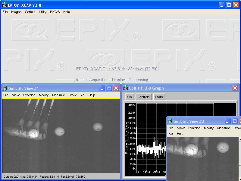
4.2. Open PIXCI® Frame Grabber
XCAP is normally configured to automatically open the PIXCI® frame grabber for use and show the PIXCI® Image Viewer window.
Alternately, in the XCAP Main Window, click:
    PIXCI®
    PIXCI® Open/Close
A dialog window appears.
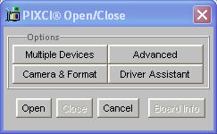
Clicking:
Open
opens the PIXCI® frame grabber for use, removes the Open/Close
dialog.
Upon opening selected PIXCI® frame grabbers, XCAP may display a Camera & Format dialog listing various compatible cameras. Simply click:
    .. select camera from list ..
    OK
    Open
Opening the PIXCI® frame grabber creates a PIXCI® Image Viewer window showing the first PIXCI® frame buffer, creates a Capture & Adjust dialog with commonly used camera and video capture adjustments, and creates a Shortcuts Toolbar for accessing the most commonly needed features.
The following windows are now active:
- The Main Window, which has options for reconfiguring the PIXCI® frame grabber, and has features independent of the PIXCI® frame grabber, such as loading images into image buffers unrelated to video capture hardware.
- The PIXCI® Image Viewer window, from which the PIXCI® frame buffers are captured, viewed, examined, processed, measured, and saved, with a status bar below the image with cursor coordinates, video frame rate, and other information.
- The PIXCI® Shortcut Toolbar, with shortcuts for the most commonly needed features relating to the PIXCI® frame grabber and its frame buffers. The Shortcuts may appear within the PIXCI® Image Viewer window, to the left of the image, rather than a separate window.
- A Capture & Adjust dialog, with commonly used camera specific (as appropriate for that specific frame grabber) and video capture adjustments.
XCAP may have been configured for one or more variations, such as, (a) Automatically opening, or not opening, the PIXCI® frame grabber and displaying the PIXCI® Image Viewer, (b) Eliminating the Main Window with its menus integrated into the PIXCI® Image Viewer window, (c) Configuring the Shortcuts and/or Capture & Adjust features to be attached to the PIXCI® Image Viewer window rather than detached in their own windows, (d) Selecting whether the Shortcuts and/or Capture & Adjust features appear automatically, or only when:
    Capture
    Shortcuts
or
    Capture
    Adjustments
are clicked, or (e) Removing the status bar to increase the
screen area available for image display. These variations allow
custom configuration of XCAP, but do not affect the functionality
of the Shortcuts or Adjustments features.
4.3. PIXCI® D, D24, D32, D2X, D3X Video Configuration
The PIXCI® D, D24, D32, D2X, and D3X frame grabbers are customized for a specific camera. XCAP identifies the specific PIXCI® D, D24, D32, D2X, and D3X frame grabber, and typically defaults, for area scan cameras, to capturing full video resolution from the specific camera.
Selected PIXCI® D, D24, D32, D2X, and D3X frame grabbers may be compatible with two or more related cameras. To select a different compatible camera, from the Main window, click:
    PIXCI®
    PIXCI® Open/Close
    Close (if open)
    Camera & Format
    .. select camera from list ..
    OK
    Open
4.4. Capturing Images
Once the PIXCI® frame grabber is opened for use, images can be captured from the PIXCI® Image Viewer, by clicking:
    Capture
    Snap
or
    Capture
    Live
The Snap captures a single image into the current frame
buffer, while Live continuously captures images into the current frame
buffer and continuously updating the image shown on the graphics
display.
The Live mode can be used to adjust the camera's focus, aperture, and position. The Live mode can be halted by clicking:
    Capture
    UnLive
A Live
followed immediately by
Unlive has the same effect as Snap, assuming the camera is in the most-common, free-run
mode.
If the current video resolution and frame buffer memory size allows more than one frame buffer, clicking:
    Capture
    Adjustments
provides the:
Current (Frame) Buffer: 0
which may be incremented or decremented at any time, whether in
Live
or UnLive mode. The window reached by clicking:
    Capture
    Adjustments
has convenient buttons that duplicate the Snap, Live, and UnLive
features.
As three of the most commonly used operations, the Snap, Live, and UnLive are also available in the Shortcuts Toolbar, as two shortcuts with a graphic of camera; one for snap and the other for live/unlive. The Shortcuts also allow changing the current frame buffer, as four shortcuts with the graphic of a book's pages; switch to the first frame buffer, to the next frame buffer (e.g. current buffer +1), to the previous frame buffer (e.g. current buffer -1), and to the last frame buffer. The relative position of these shortcuts changes depending on whether the Shortcuts Toolbar is standalone window or within the PIXCI® Image Viewer window, and depending on the graphic display resolution and size of the windows; hovering the mouse over the shortcuts will explain the use of each.
4.5. Examining Images
4.5.1. Altering How the Image is Displayed
The PIXCI® Image Viewer can be moved and resized, using standard techniques (drag the window's title bar, drag the window's corner, etc). By default, the captured image is displayed with resizing, so that the entire image fits within the Image Viewer.
For many engineering and scientific applications, examination of individual pixel values is critically important. Resizing the image may ''hide'' defective pixels; resizing an image with interlace jitter may turn odd/even line striping into bars of striping.
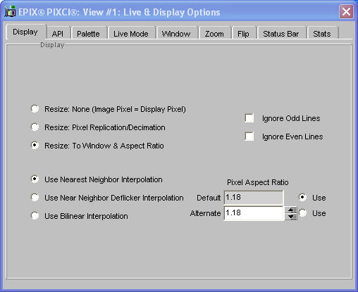
To view pixels without resizing artifacts, from the PIXCI® Image Viewer, click:
    View
    Display
    Resize: None (Image Pixel = Display Pixel)
Each image pixel is now displayed as exactly one graphics display
pixel. Of course, depending upon the image resolution, graphics
display resolution, and window size, the entire image may not fit.
If the image doesn't fit, then (a) Scroll bars appear,
allowing the viewed portion of the image to be panned and scrolled
throughout the entire image, and (b) Moving the mouse with
right button held over the displayed image causes panning or
scrolling (if there is more image to be seen in the direction the
mouse is moving).
For high resolution displays and lower resolution images, using:
Resize: Pixel Replication/Decimation
will provide a more pleasing display; duplicating pixel values to
fill the display while still avoiding resizing artifacts.
For cameras that don't have square pixels (i.e. aspect ratio), after selecting:
Resize: None (Image Pixel = Display Pixel)
or
Resize: Pixel Replication/Decimation
the displayed image's aspect ratio may not appear correct; the
aspect ratio can't be corrected without some form of resizing or
resampling! To display the image with the correct aspect ratio,
choose:
Resize: To Window & Aspect Ratio
4.5.2. Zoom, Mirror, Flip
To magnify the displayed image, from the PIXCI® Image Viewer, click:
    View
    Zoom, Pan, Scroll
    Zoom On
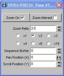
Zoom Ratio
Or, if
Zoom Interact
is enabled, magnification can be increased or decreased by clicking
on the image. When magnified, only a portion of the image is
visible. As described above, the viewed portion may be panned and
scrolled through the entire image with the scroll bars, or by
moving the mouse over the image with right button held.
Alternately, to use ''spot'' magnification in XCAP-Plus, XCAP-Std, or XCAP-Ltd, from the PIXCI® Image Viewer, click:
    Examine
    Pixel Magnifier
The magnification factor can be adjusted with:
Magnification
The ''spot'' size and shape can be adjusted with:
    Magnifier Size
    Square
vs  Circle
The ''spot'' position can be moved interactively by clicking:
Coord<=>Cursor
A cursor now appears over the image window; clicking the mouse on
the image window moves the cursor to that position, and spot
magnifier to be centered on that position.
To re-orient the displayed image on to its side or top, or to mirror the displayed image, from the PIXCI® Image Viewer, click:
    View
    Flip & Mirror
and select an up, down, left or right orientation and select one of
two mirror options.
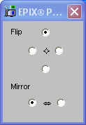
4.5.3. Numeric Pixel Values
To examine numeric values of pixels as a table, from the PIXCI® Image Viewer, click:
    Examine
    Pixel Peek
A table of pixel values for a portion of the image appears, showing
pixel values in the neighborhood of the displayed X and Y
coordinates. The portion of the image numerically displayed can be
moved by using the scroll bars, or by entering new X and Y
coordinates.
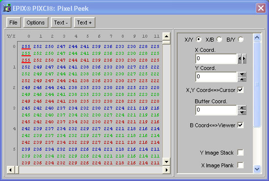
The portion of the image which is numerically displayed can also be moved interactively by clicking:
Coord<=>Cursor
A cursor now appears over the image window (the Pixel Peek window
may have to be moved to the side so that both the pixel peek window
and the image viewer window can be seen); clicking the mouse on the
image viewer window moves the cursor to that position, and
repositions the numerically displayed portion of the image to be
centered at that position.
To examine pixel values as a two-dimensional graph, click:
    Examine
    Pixel Plot
and
    Controls
    Where
and Plot Row
or  Plot Column
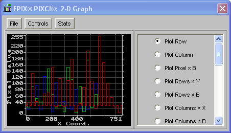
Coord<=>Cursor
A cursor now appears over the image window; clicking the mouse on
the image window moves the cursor to that position, and repositions
the displayed line (column) to that Y (X) coordinate.
4.6. PIXCI® D, D24, D32, D2X, D3X Video Adjustments
4.6.1. Video Resolution
For area scan cameras, reducing the video resolution (the number of pixels captured per line and column) allows capturing more video frames in a given size of frame buffer memory. From the PIXCI® Image Viewer, click:
    Capture
    Adjustments
    Res(olution)
Click:
Set Video Window
and draw the new desired area to be captured by left clicking and
dragging over the displayed image. Click:
OK
to accept the new capture resolution. Note: Changing the capture
resolution will destroy any images previously captured in the frame
buffers!
For line scan cameras, the number of scanned lines which compose each two-dimensional image can be set: From the PIXCI® Image Viewer, click:
    Capture
    Adjustments
    Res(olution)
Set the:
Lines per Field
to the desired number.
The
    Capt(ure)
    Frame Buffers
shows the number of frame buffers available with the current
selections.
4.6.2. Saving the Video Configuration
The selections under the PIXCI® Image Viewer:
Adjustments
are automatically saved when the PIXCI® frame grabber is
closed, and/or XCAP is exited. When the PIXCI® frame grabber is
next opened, clicking (from the XCAP Main Window):
    PIXCI®
    PIXCI® Open/Close
    Camera & Format
Choose:
Open w. last used Video Setup
to use the previous video setup, or choose:
Open w. default Video Setup
to start afresh with the default video format and resolution.
4.6.3. Camera Controls
Most of the supported cameras provide controls and features above and beyond sending imagery to the PIXCI® frame grabber. For most cameras, these controls are either switches on the back of the camera, or commands sent through an RS-232 port.
XCAP integrates controls for either type of camera within the Capture & Adjust window. The left side of the Capture & Adjust window contains controls for the PIXCI® frame grabber. The right side of the Capture & Adjust window provides camera specific controls; these utilize the same concepts and terminology as specified by the camera's manufacturer, so that the camera manufacturer's documentation can be directly applied to these features and controls.
For cameras with switches, the camera's settings can neither be set nor sensed by XCAP! Instead, the Capture & Adjust window shows a sketch of the camera's controls. After selecting a camera operating mode by setting the camera's switches, adjust the sketch's controls to match those of the camera. This convenient technique advises XCAP of the camera's configuration, and allows automatically setting the PIXCI® frame grabber's configuration to match.
For cameras with RS-232 controls, connect the camera's RS-232 connector to the computer's RS-232 (aka ''COM'') port. In the Capture & Adjust window, use:
RS-232 Port
to select the connected ''COM'' port (under Windows) or ''ttyS''
device (under Linux). Thereafter, any change of the camera's
controls shown in the Capture & Adjust window simultaneously
programs the camera and automatically sets the PIXCI® frame
grabber's configuration to match! There is no need to run the
camera manufacturer's separate RS-232 control program.
4.6.4. Color Cameras
For color cameras with so-called ''Bayer format output'', it is XCAP software which performs color adjustments and white balancing, not the camera. From the PIXCI® Image Viewer, click:
    Capture
    Adjustments
    Color (or Clr)
For most common conditions:
- Select one of the pre-defined correlated color temperatures, either based on best appearance, or matching the color temperature of the current illumination. The 5000°K selection is average overcast daylight, the 4100°K selection is a typical cool white fluorescent bulb, and the 2800°K selection is a typical 60 to 100 watt tungsten bulb.
- Choose one of the predefined color qualities, trading quality for speed.
- If none of the predefined settings is satisfactory, start with
the best setting and click:
Cover the camera's lens and click:Customize
Finally point the camera at a white target (but preferably not a target using fluorescent brighteners) and click:Black BalanceWhite Balance
4.7. Saving Images
To save a captured image, from the PIXCI® Image Viewer, click:
    File
    Save Image
Choose a file format, such as:
    TIFF
    BigTIFF
    BMP
    FITS
    JPEG/JFIF
    Portable Map
    X/Y Binary
    X/Y ASCII
The JPEG/JFIF and Windows BMP formats have near-universal support
among graphics and imaging applications, with support for 8 bit
monochrome and 24 bit RGB color; JPEG/JFIF provides ''lossy''
compression, with adjustment for image quality versus file size.
The TIFF format has near-universal support among imaging
applications supporting a wide variety of pixel formats and bit
depth; TIFF is suggested for saving and reloading an image into
XCAP, and suggested for exporting images to other applications. The
BigTIFF format is variation of TIFF allowing file sizes larger than
4 Gbyte; however it is not commonly supported. Both TIFF and
BigTIFF offer options for lossless compression. The FITS format is
commonly used within the astronomy community.
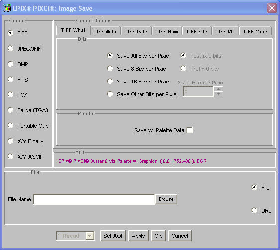
The X/Y Binary and X/Y ASCII export raw pixels, left to right, top to bottom, with no excess information such as dimensions, bit depth, date, format, etc; these are useful for exporting images to a spreadsheet (X/Y ASCII), or to your own program in which the image's dimensions are assumed and can simply read a 2-D array of values. The Portable Map also exports raw binary pixels, left to right, top to bottom, but with minimal information, such as dimensions, at the start of the file.
After selecting a file format, enter a file name:
File Name: xx.tif
and click
OK
to save the image. Or, use the:
Browse
button to access the standard Windows or Linux File Dialog, click
Accept
to accept the filename selected by browsing, and click
OK
to save the image.
4.8. Capturing an Image Sequence
To capture an image sequence into the frame buffers:
    Capture
    Sequence Capture
    Video to Frame Buffers
select:
Start/End All Buffers
to capture into all of the frame buffer memory,
Capture Video Fastest
to capture each video frame (rather than intentionally skipping
frames),
Linear Sequence
to capture into each frame buffer once, then stop (rather than
capturing continuously, reusing frame buffers until explicitly
stopped),
Event Free
to capture without waiting for additional events, and and click:
Record
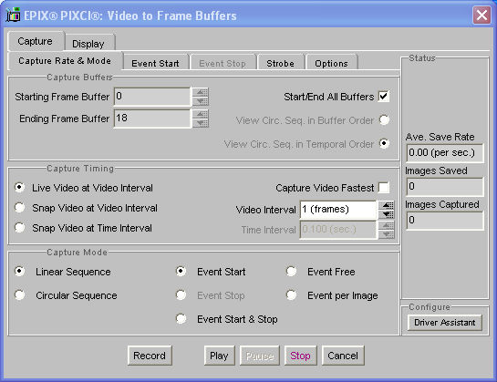
The VideotoFrameBuffers captures into frame buffer memory; to request more frame buffer memory and a thereby a longer sequence use the
Driver Assistant
A variety of Sequence Capture features are available, providing tradeoffs between capture rate vs. convenience vs. total number of images captured. The Video to Frame Buffers captures sequences directly into pre-configured frame buffer memory, and can support the maximum frame rate. The Video to Virtual Memory captures and copies sequences into host computer (virtual) memory which is conveniently allocated as-needed, but may not support maximum frame rate capture for all cameras on all computers. The Video to Disk File captures and copies sequences into a disk file in an efficient, internal format (after capture the sequence can be saved in a standard format), but frame rate is limited by the bandwidth of the computer and disk subsystem.
The Video to Image Files captures and copies sequences directly into standard format image files, but with more overhead than the Video to Disk File feature. Optionally, each captured image can also be saved offsite directly to an FTP URL. Optionally, the HTTP server (i.e. web server) feature of XCAP allows access to the sequence of images - as they are being captured - via an internet web browser.
4.9. Saving Image Sequences
To save a captured image sequence, from the PIXCI® Image Viewer, click:
    File
    Save Image Sequence
Choose a file format, such as:
    One TIFF w. Sequence
    One AVI/DIB w. Sequence
    One AVI/MJPG w. Sequence
    One BigTIFF w. Sequence
    One FITS w. Sequence
    One Portable Map w. Sequence
    One X/Y Binary w. Sequence
    One X/Y ASCII w. Sequence
    Sequence of BMP's
    Sequence of BigTIFF's
    Sequence of FITS's
    Sequence of JPEG/JFIF's
    Sequence of TIFF's
    Sequence of Portable Map's
    Sequence of X/Y Binary's
    Sequence of X/Y ASCII's
The One TIFF, One BigTIFF, One FITS, One Portable Map One X/Y
Binary, and One X/Y ASCII w. Sequence save the entire image
sequence into a single file, with similar utility as described
above for the corresponding file format.
The One AVI/DIB and One AVI/MJPG w. Sequence save the entire image sequence as one Windows AVI file using a ''DIB'' or a ''MJPG'' codec, respectively; essentially multiple BMP or multiple JPEG/JFIF formated images, respectively, with the same supported bit depth and compression options described above.
The other options save each image as an individual file.
Only the One TIFF q. Sequence format and the Sequence of ... formats are available in XCAP-Lite.
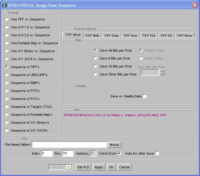
After selecting any of the ''One .. w. Sequence'', file formats, enter a file name:
File Name: xx.tif
and click:
OK
to save the image(s). Or, use the:
Browse
button to access the standard Windows or Linux File Dialog, click:
Accept
to accept the filename selected by browsing, and click:
OK
to save the image(s).
If using any of the ''Sequence of ..'' file formats, enter a file name pattern:
File Name: xx???.tif
where the ''?'' characters will be replaced by a numerical index,
(enter sufficient ''?'' characters as per sequence length; three
''?'''s are sufficient for 1000 images) and click:
OK
to save the image(s).
4.10. Additional XCAP Documentation
For additional guidance in using XCAP, click
    Help
    XCAP Reference Manual
to browse the full manual.
5. XCAP Software Guide
XCAP is a family of sophisticated, interactive, imaging programs specifically designed to support the PIXCI® series of frame grabbers, but also able to process and analyze images from other imaging sources. Several versions of XCAP are available: XCAP-Plus, XCAP-Std, XCAP-Ltd, XCAP-Lite, and XCAP-Viewer. All versions share the same user interface and menu structure, but selected features in XCAP-Std, XCAP-Ltd, XCAP-Lite, and XCAP-Viewer are not operational. XCAP is distributed on CD/DVD, or downloadable from the EPIX, Inc. website. After installation, a 12 character activation or ID code[6] is entered to configure XCAP as either XCAP-Plus, XCAP-Std, XCAP-Ltd,[7] or XCAP-Lite; or, lacking a valid activation or ID code, configured as XCAP-Viewer.
XCAP-Std is an interactive, imaging program designed for scientific, industrial, and machine vision applications. XCAP-Std supports the PIXCI® frame grabber, providing video format and resolution configuration; continuous (live), video rate sequence, and triggered capture; and single or sequence, zoomed or resized, display. The image frame buffers of PIXCI® frame grabbers can be loaded, examined, processed, analyzed, measured, printed, annotated, and saved.
XCAP-Std also allows loading, analyzing, modifying, and saving a pre-existing image or image sequence with size, pixel depth, and color space independent of the PIXCI® frame grabber's configuration; XCAP-Std can be used with pre-existing images even when the PIXCI® frame grabber is not present. XCAP-Std can also acquire images from TWAIN compliant devices.
XCAP-Plus provides extra, advanced, features in addition to all of the capabilities of the XCAP-Std, such as support for specialized, optional, hardware.
XCAP-Ltd is a simplified version of XCAP-Std. XCAP-Ltd provides the same image acquisition and PIXCI® frame grabber control capabilities, the same image display features, and the same image loading, examining, printing, and saving of single image or sequences of images. Only minimal image processing, measurement, analysis, and scripting features are functional. XCAP-Ltd can be used with pre-existing images even when the PIXCI® frame grabber is not present.
XCAP-Lite is a much simplified version of XCAP-Std. XCAP-Lite provides similar image acquisition and PIXCI® frame grabber control capabilities, video format and resolution configuration; continuous (live), video rate sequence, and triggered capture; and single or sequence, zoomed or resized, display. XCAP-Lite also provides some of the image loading, examining, printing, and saving features, but minimal processing, measurement, analysis, and scripting features are functional. XCAP-Lite allows loading and saving single images, as well as image sequences in TIFF format.
XCAP-Viewer allows browsing through the dozens of processing, measurement, analysis, and graphics features provided in XCAP-Plus, XCAP-Std, XCAP-Ltd, or XCAP-Lite. XCAP-Viewer can load and display pre-existing single images. The PIXCI® frame grabber can't be operated with the XCAP-Viewer version.
As XCAP-Plus, XCAP-Std, XCAP-Ltd, XCAP-Lite, and XCAP-Viewer share many common features, this manual typically refers to all versions as XCAP, except where explicitly differentiated.
The XCAP features are organized into two major types of windows, the Main Window and one or more Image Viewer Windows.
For each image, or sequence of images, an Image Viewer Window shows that image, or a selected image of that sequence, and via its menu bar allows viewing, examining, processing, analyzing, or drawing upon that image (sequence). The Image Viewer Window associated with the PIXCI® frame grabber's frame buffers also provides features for capturing new images. There can be multiple Image Viewer Windows for the same image (sequence), allowing, for example, viewing the image both magnified (i.e. zoom) and unmagnified, or simultaneous viewing of different images of a sequence.
The Main Window allows creating new image (sequences), and thus new Image Viewer Windows, either by loading a new image from file, explicit specification of the new image's dimensions, or by opening the PIXCI® frame grabber for use. Video setup for the PIXCI® frame grabber, such as modifying the video resolution or color space, are also in the Main Window; these features may close and re-create the PIXCI® frame grabber's Image Viewer Window. The Main Window also provides features not directly associated with an image (sequence), such as scripts, RS-232 device control, and features to customize XCAP.
5.1. The Main Window
The XCAP main window provides a menu bar with File, Images, Scripts, Utility, PIXCI®, and Help features.
5.1.1. Main Window - File
The main window's File allows loading of pre-existing images into new image buffers, displaying attributes about pre-existing images, and acquiring images from TWAIN compliant devices.
The Load New Image and Load New Image Sequence creates a new image buffer (sequence) with dimensions, pixel depth, and color space matching a specified AVI (Audio Video Interleaved), BigTIFF (Tagged Image File Format extended for large file sizes), BMP (Bitmap), FITS (Flexible Image Transport System), JPEG (Joint Photographic Exports Group), PBM/PGM/PBM (Portable Bit/Gray/Pixel Map), TIFF (Tagged Image File Format), VIF (Video Frame Files - Video to Disk) or multimedia format file(s), and loads the image(s) from the file(s). This feature, and the image buffer (sequence) created, is unrelated to the PIXCI® frame grabber's frame buffers. After creation and loading, the new image (sequence) is displayed, processed, and analyzed in a new instance of The Image Viewer Window, described below. Using wild cards, the Load New Image can also load multiple image files - each to their own new image buffer.
The Image File Info displays information about a specified AVI, BigTIFF, BMP, FITS, JPEG, PBM/PGM/PPM, TIFF, or VIF format file without loading the image. The information displayed includes the image's dimensions, pixel depth, color space, palette option, and other file format specific information.
The TWAIN Select Source and TWAIN New Acquire allow using XCAP as a TWAIN Application, acquiring images from TWAIN compliant imaging devices (TWAIN Sources). The TWAIN Select Source allows selecting which TWAIN Source is to be used, and the TWAIN New Acquire allows acquiring one image from the TWAIN Source.
The Window List displays a list of active windows belonging to XCAP; selecting a window causes that window to appear, if previously hidden, and/or to appear over other windows (subject to the priority of selected windows to always appear ''on top'').
5.1.2. Main Window - Images
The main window's Images allows creating new image buffers and activating any existing image windows that may not be on-screen.
The New Image creates a new image buffer, or sequence of image buffers, with specified dimensions, pixel depth, color space, and palette. This feature, and the image buffer created, is unrelated to the PIXCI® frame grabber's frame buffers. After creation, the new image is displayed in a new instance of The Image Viewer Window, as described below.
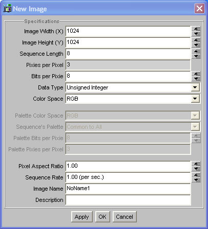
Underneath New Image are listed all existing image windows, whether for PIXCI® frame grabber frame buffers, or for independent image buffers. (The image window for PIXCI® frame grabber frame buffers appears only after the PIXCI® frame grabber has been opened for use, see below). An image window which has been closed and is thereby off-screen can be reactivated by clicking the image window's name.
5.1.3. Main Window - Scripts
The main window's Scripts provides features for recording and playing scripts. A script recording contains most of the user's interactions with the windows of XCAP; playing the script duplicates the original actions.
Some user actions are not recorded. Using the mouse to drag the cursor or other graphic across an image is not recorded as these actions are highly dependent upon image content (such as the typical scenario of dragging the cursor until it is positioned next to an artifact in a captured image), would likely be inappropriate to other captured images, and recording each mouse ''step'' would consume a significant amount of disk space. Instead, after positioning the cursor interactively the user can record the final position by clicking the appropriate numeric cursor coordinates. Similarly, the activation of a feature with shortcut keys or shortcut icons is not recorded; instead features can be activated via the non-shortcut alternative, which is recorded.
A recorded script is in a human readable form and can be altered with any common editor capable of handling ASCII text, allowing scripts to be modified or combined. A selected script may be executed automatically after XCAP starts, this feature is set in Utility, Program Setup, Startup Script.
The Load Tool Bar provides one or more user-defined tool bars of shortcuts, each shortcut represented by an icon which, when clicked, executes a user-specified script. Each shortcut may also specify an optional keyboard key which, when pressed, also executes the user-specified script.
The Script Remote Control allows using XCAP as a hidden, off-screen, ''black box''; any end-user application that can manipulate text files, can also remotely control XCAP.
5.1.4. Main Window - Utility
The main window's Utility provides an assortment of features that are of secondary importance; features that allow fine tuning of XCAP, or features needed in relatively few circumstances.
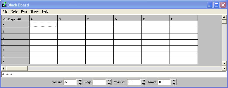
The Black Board allows customizing XCAP, creating non-procedural programs, and collecting data. The black board allows inter-connecting the numeric and text field of other windows; computed results, such as center-of-mass, may be written onto the black board - parameters for other features, such as the coordinates of a displayed grid, may be extracted from the black board - combining these automatically repositions the grid as the center of mass is recomputed! Other features allow computed values (similar to a spreadsheet), ''push''ing buttons, timed updates, creating a report to file or an RS-232 port, collecting data, and graphing the black board's contents.
A Message Log window lists warnings and errors that arise from performing various operations. By default, the message log window appears automatically when a message is added, and disappears a few seconds later. Auto appearance, auto hide, and audible clicks can be disabled (from the message log window's menu bar). The menu-bar's Message Log allows explicit activation of the message log window.
The Program Setup shows information about the installed XCAP components, such as their revision level, and sets various configuration options. For versions of XCAP that require an authorization key, it also shows the ID of the key required by the instant copy of XCAP.
The Program Setup allows specifying the name of a script to be executed when XCAP starts, whether warning pop-up windows (if any) are to be shown, whether previously saved settings are to be loaded, and other similar initial or terminal conditions.

The Program Setup also enables user-defined translation of XCAP labels and messages for use in non-English speaking countries.
The Windows Info displays information about the current Windows environment, such as memory usage and the graphics display system's features, as reported by Windows.
The Window Style allows setting some characteristics of XCAP windows, such as color or character size and font. Some characteristics of window style are instead controlled by the Windows Control Panel.
The Audio Clip (only under Windows) allows recording and playing short audio ''clips''.

The RS-232 Terminal allows ''raw'' communication with a camera or other device connected via the computer's RS-232 port. The RS-232 Terminal is designed specifically for device control, including options to communicate with byte values, rather than as a common ''terminal emulator''. XCAP may also provide more convenient, camera-specific ''smart'' controls, provided after a camera-specific frame grabber is opened, via the Capture - Adjustments.
The I/O Port Peek & Poke allows controlling arbitrary devices accessible via I/O port peeks and pokes. This feature must be used with caution; peeking or poking arbitrary ports will cause computer malfunction! This feature is only available under Windows 95, 98, and ME.
The Screen Capture allows capturing the current graphics display screen, saving the graphics to a file, or printing the graphics. The Screen Capture also allows capturing numeric and textual parameters into a text file, suitable for loading into a spreadsheet or other programs.
The Volpi intralux dc-1100 and Illumination Technologies 3900 provide support for controlling these light sources through their RS-232 ports.
The Birger EF232 provides support for controlling the Birger EF232 RS-232 Lens Mount.
The Fujinon CCTV Lens provides support for controlling Fujinon CCTV Lenses that follow the Fujinon C10 Protocol.
The Directed Perception Pan-Tilt Unit provides support for controlling the Directed Perception Pan-Tilt Units.
The Sagebrush Pan-Tilt Gimbal provides support for controlling the Sagebrush Pan-Tilt Gimbals that follow the Sagebrush 2.0 Protocol.
The EPIX® SILICON VIDEO® 20C-CL, EPIX® SILICON VIDEO® 20M-CL, EPIX® SILICON VIDEO® 1514CL, and EPIX® SILICON VIDEO® 1820CL provide support for configuring the EPIX® SILICON VIDEO® 10C-CL, SILICON VIDEO® 10M-CL, SILICON VIDEO® 20C-CL, SILICON VIDEO® 20M-CL, SILICON VIDEO® 1514CL, and SILICON VIDEO® 1820CL cameras via a virtual ''COM'' port (under Windows), a virtual ''ttyS'' device (under Linux), or a Camera Link Serial API DLL (i.e. a clserXXX.DLL, under Windows). These are provided for configuring the camera when using a frame grabber other than an PIXCI® frame grabber, leaving configuration of the frame grabber to its software. When using a PIXCI® frame grabber, the alternative PIXCI® - Open/Close is recommended as it provides integrated controls for both camera and frame grabber.
5.1.5. Main Window - PIXCI®
The main window's PIXCI® allows initiating access to the PIXCI® frame grabber and provides configuration options. Actual operation of the PIXCI® frame grabber is performed through the PIXCI® image viewer window's menu-bar.
The PIXCI® Open/Close allows opening access to, or closing access to, the PIXCI® frame grabber. Once open, the model, and submodel or preset camera & format selection, as appropriate, of the PIXCI® frame grabber is available via the Board Info button. After opening, the contents of the PIXCI® frame grabber's image frame buffer(s) are displayed in a new instance of The Image Viewer Window, along with a tool bar of PIXCI® Image Viewer - Capture - Shortcuts and a status bar of Image Viewer - View - Status Bar are shown as described below.
The PIXCI® Video Setup allows configuring the video format, video resolution and other, model specific, video characteristics. For the PIXCI® SV2, SV3, SV4, SV5, SV5A, SV5B, and SV5L models, the PIXCI® Video Setup allows selecting NTSC, RS-170, NTSC/S-VIDEO, CCIR, PAL, or PAL/S-Video formats, allows selecting the video window size, capture resolution, and other video acquisition characteristics.
For the PIXCI® SV7 models, the PIXCI® Video Setup allows selecting NTSC, RS-170, CCIR, or PAL formats , allows selecting the video window size, capture resolution, and other video acquisition characteristics.
For the PIXCI® SV8 models, the PIXCI® Video Setup allows selecting NTSC, RS-170, NTSC/S-VIDEO, CCIR, PAL, or PAL/S-Video formats, allows selecting the video window size, capture resolution, and other video acquisition characteristics.
For the PIXCI® A310 model, the PIXCI® Video Setup allows selecting Video 720x480i 60Hz (RS-170), Video 720x480i 60Hz RGB, Video 720x576i 50Hz (CCIR), Video 720x576i 50Hz RGB, Video 1920x1080i 60Hz, Video 1920x1080i 60Hz RGB, Video 1920x1080i 50Hz, Video 1920x1080i 50Hz RGB, Video 1920x1080p 60Hz, Video 1920x1080p 60Hz RGB, Video 1920x1080p 50Hz, Video 1920x1080p 50Hz RGB, Video 1280x720p 50Hz, Video 1280x720p 50Hz RGB, Video 1280x720p 60Hz, Video 1280x720p 60Hz RGB, RS330 720x480i 60Hz, RS343 875i 60Hz, RS343 875i 60Hz RGB, SVGA 800x600 60Hz, SVGA 800x600 60Hz RGB, SXGA 1280x1024 60Hz, SXGA 1280x1024 60Hz RGB, VGA 640x480 60Hz, VGA 640x480 60Hz RGB, XGA 1024x768 60Hz or XGA 1024x768 60Hz RGB formats, allows modifying the PLL, A/D, and sync processor parameters to accommodate other video formats, allows selecting the capture resolution, and selecting other video acquisition characteristics. For the PIXCI® A110 model, the PIXCI® Video Setup is similar, but does not allow selecting RGB formats.
For the PIXCI® CL1, CL3SD, D, D24, D32, D2X, D3X, and D3XE models, fewer options are provided, as these frame grabbers are each customized to specifically support one camera, or a related group if cameras. For the PIXCI® CL2, E1, E1DB, E4, E4DB, E4G2-2F, E4G2-4B, E4G2-F2B, E4TX2-2F, E4TX2-4B, E4TX2-F2B, E8, E8DB, e104x4-2f, e104x4-4b, e104x4-f2b, EB1, EB1G2, EB1-PoCL, EB1G2-PoCL, EB1mini, miniH2B, miniH2F, miniH2x4F, mf2280, EC1, ECB1, ECB1-34, ECB2, EL1, and EL1DB models, which provide universal support for Camera Link cameras, fewer options are provided. For the PIXCI® E8CAM, ELS2, SI, SI1, SI2, and SI4 models, which support SILICON VIDEO® cameras, fewer options are provided. For all of these, a different camera can be selected, if available, via PIXCI® Open/Close, Camera & Format.
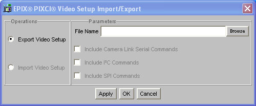
The current video setup is automatically saved when access to the PIXCI® frame grabber is closed, and reloaded when the PIXCI® frame grabber is later opened. The PIXCI® Export Video Setup and PIXCI® Import Video Setup may be used to explicitly save or reload the current video setup, such as to choose amongst several favorite setups, or to export the current video setup to the XCLIB library.
The PIXCI® Status shows the PIXCI® frame grabber's current status, such as the state of the general purpose (formerly referred to as an external TTL) trigger input(s) and output(s), the number of elapsed video fields, the board's model, submodel or preset camera & format selection, as appropriate, and configured image memory size.
The PIXCI® Serial Terminal allows ''raw'' communication with a camera connected to the serial port on selected models of the PIXCI® frame grabber. For many cameras, XCAP includes more convenient, camera-specific ''smart'' controls, provided after a camera-specific frame grabber is opened, via the Capture - Adjustments.
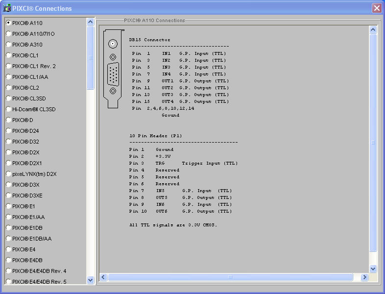
The PIXCI® Connections provides, as appropriate for the specific model of PIXCI® frame grabber, a map of the board's connections, connectors, option jumpers, and adjustments.
The PIXCI® Camera Info provides a list of cameras and video formats supported by XCAP and various PIXCI® frame grabbers. The PIXCI® Camera Info also allows viewing a non-operational Capture - Adjustments window (i.e. the ''Control Panel'', which provides integrated control of both frame grabber and any supported camera).
The PIXCI® TWAIN Sourcery (only under Windows) allows using XCAP, in conjunction with the ''XCAP Sourcery'' TWAIN driver, as a component of a ''smart'' TWAIN Source, allowing other applications to capture images from the PIXCI® frame grabber, while XCAP provides frame grabber controls, camera controls, and, optionally, image preprocessing.[8] The PIXCI® TWAIN Sourcery should not be confused with TWAIN New Acquire; the former allows XCAP to provide image data to other, TWAIN compliant applications; the latter allows XCAP to accept image data from other TWAIN compliant sources. The TWAIN New Acquire should never be used to attempt to acquire image data from the PIXCI® TWAIN Sourcery!
The PIXCI® Image-Pro Sourcery (only under Windows) allows using XCAP, in conjunction with the ''XCAP Sourcery'' Image-Pro driver, as a component of a ''smart'' video source, allowing Image-Pro to capture images from the PIXCI® frame grabber, while XCAP provides frame grabber, camera controls, and, optionally, image preprocessing.[8]
5.2. The Image Viewer Window
Each image buffer (sequence), or frame buffer (sequence), is displayed in an image viewer window, which is the focus of activity for examining, processing, or analyzing that image buffer (sequence). The image viewer window provides a menu bar with File, View, Examine, Modify, Measure, Draw, AOI, and Help features. The image viewer window associated with the PIXCI® frame grabber's frame buffer(s) also provides a Capture feature.
5.2.1. Image Viewer - File
The image viewer window's File allows saving, loading, or printing the image, shows information about the image's dimensions, pixel depth and color space, and allows closing the image viewer window.
The Load Image and Save Image allow saving or loading the image in a variety of file formats. The Load Image, unlike the Load New Image described above, loads an image file into the current image buffer, resizing and/or color converting to fit the image buffer's existing dimensions, pixel depth, and color space. The Load Image can also load images directly from an Internet URL.
For image viewer windows associated with an image buffer sequence, the Save Image Sequence and Load Image Sequence allow saving or loading multiple images of the sequence as a numbered sequence of image files, or as a single AVI, BigTIFF, FITS, PBM/PGM/PPM, or TIFF format image file with multiple images. Save Image can also save images directly to an FTP URL.
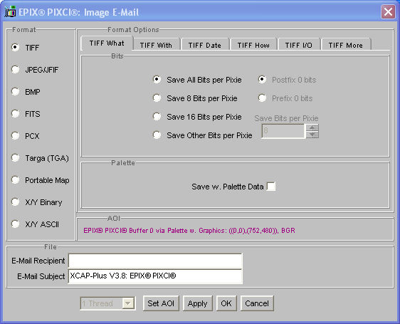
The E-Mail Image allows directly e-mailing the image, in a variety of file formats, from within XCAP.
The Print Image allows printing the image; either via the operating system's built-in image printing feature(s) which typically supports a wide variety of printers, or via EPIX® imaging drivers which support only the most popular printers, but providing precise control of print options.
The Image Attributes shows the image's (or image sequence's) dimensions, pixel depth, and color space.
The Duplicate Image and Duplicate Image Sequence allows creating a new image buffer and copying the current image, or creating a new sequence of image buffers and copying the current image sequence, respectively, in one step. It optionally allows copying the image's (or image sequence's) current appearance, as modified by the palette and graphics, instead of the underlying image (or image sequence).
The BlackBoard Image allows copying the image's pixel values into the Black Board.
The Close Viewer closes the window, but does not destroy the image (sequence). The Close & Dispose of Image closes the window and destroys the image (sequence). The image viewer window associated with the PIXCI® frame grabber's frame buffer(s) does not provide a Close & Dispose of Image; an image viewer window is available whenever the PIXCI® frame grabber is open for use.
5.2.2. Image Viewer - View
The image viewer window's View provides options governing the appearance of the displayed image.
The Shortcuts allows activating or deactivating a tool bar of icons providing shortcuts for accessing often used features, and is described under Image Viewer - View - Shortcuts.
The Status Bar allows activating or deactivating a small status bar with current information, and is described under Image Viewer - View - Status Bar.
The Menu Bar allows activating or deactivating the menu bar; when deactivated, clicking the mouse right-click button allows restoring the menu bar.
For image viewer windows associated with the PIXCI® frame grabber's image frame buffer(s), the Adjustments allows setting common adjustments, as suitable for the model of the PIXCI® frame grabber in use, and is described under PIXCI® Image Viewer - Capture.
The Full Screen allows displaying the image in the full graphics display screen without the menu bar, centered with black border (if needed), and with little or no window ''frame'' around the image. The previous display mode can be restored via a mouse right-click.
The Always-On-Top allows forcing the image viewer window, and its subwindows, to always be ''above'' other windows; subject to the other windows' also requesting Always-On-Top, and the whims of the host operating system. This option is typically useful only when XCAP is being used in combination with other applications, such as in conjunction with the PIXCI® TWAIN Sourcery or PIXCI® Image-Pro Sourcery feature. The Always-On-Top feature is only supported under Windows.
The Refresh forces the displayed image to be redrawn once; normally manual refresh is not needed, but occasionally, when the image was (partly) covered and uncovered by other window(s), the displayed image might ''forget'' to be updated.

For images composed of index pixels and palette, the Image's Palette allows manipulating the image's attached palette; for images of other types, the Image's Palette is not selectable. For all images, the Viewer's Palette allows manipulating a palette which is not attached to the image. Either can be used for contrast enhancement, adjustment of black level and gain, or, for monochrome images, false coloring. Either, or neither, of the palettes can be selected for use under Display.
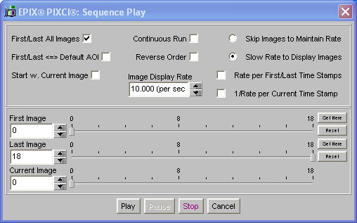
For image sequences, the Sequence Play allows ''playing'' the sequence, image by image, at a selected rate.
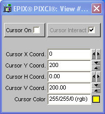
The Cursor allows activating a cursor over the image, which may be positioned via coordinates, or by left clicking the mouse on an image feature.
The Display allows selecting how the image is displayed: (a) No resizing so there is a one to one relationship between an image pixel and a displayed graphics display pixel and is the quickest, although the entire image may not fit within the window and must therefore be panned and scrolled, (b) Resize by nearest neighbor which is relatively quick, or (c) Resize by bilinear interpolation which may produce better results for continuous tone images, but is slower. For the resize modes, the aspect ratio can also be modified. The Display allows selecting which palette, if any, is to be used during display and during file loads and saves. An option to display only even lines, or only odd image lines, allows avoiding interlace artifacts during display. For the image viewer window associated with the PIXCI® frame grabber's frame buffer(s), the Display provides additional features, identical to the Live Options described below.
The Zoom, Pan, Scroll allows magnifying the displayed image, panning and scrolling to view different portions of the image under magnification. For image sequences, a specific image of the sequence can be selected for display. In addition to panning and scrolling via explicit coordinates and via scrollbars, holding the right mouse button and moving the mouse over the image also implements panning and scrolling. Optionally, the left or right mouse button can be used to increase magnification (i.e. zoom-in) or decrease magnification (i.e. zoom-out).
The Flip & Mirror allows flipping and mirroring the displayed image so that the top is displayed to the top, left, right, or bottom.
Each image buffer (sequence) may have several simultaneously active viewers, allowing, for example, viewing the same image buffer both magnified and unmagnified. The Launch 2nd Viewer creates a second image viewer window into the same image buffer (sequence), with the same features as the original image viewer window.
5.2.3. Image Viewer - Examine
The image viewer window's Examine provides options to examine the image.
The Pixel Peek allows numeric display of the pixel values in the vicinity of the image cursor — within a single image, or across a sequence of images, or of a multi-image stack. The feature also graphically displays each pixel's value or trends.
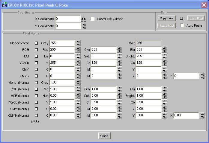
The Pixel Peek & Poke allows numeric display and modification of individual pixel values. The Pixel Peek & Poke also allows precise, single pixel, image editing.
The Pixel Plot displays a two-dimensional graph of pixels values along a selected image line or column, of all image lines or columns, of an image pixel as it varies across an image sequence, of rows or columns as they vary across an image sequence, or of a multi-image stack. The recent trends of pixel values can also be shown, as an fading ''echo,'' to help visually evaluate the fluctuations of live video or the effects of camera adjustments. Features attached to the graph show specific pixel values and descriptive statistics such as lowest value, highest value, mean value, and standard deviation.
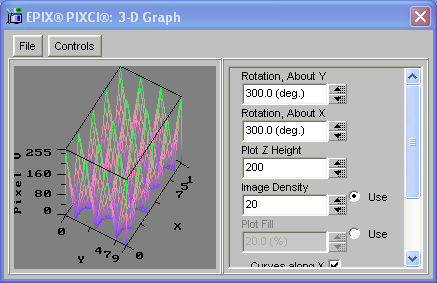
The Pixel Plot 3D displays the numeric values of pixels as as a three-dimensional graph — from a single image or from a multi-image ''stack'' — with the image X and Y coordinates composing two dimensions, and the pixel values composing the third dimension.
The Pixel Magnifier allows enlarging an area of the displayed image, with an effect similar to using a magnifying lens. Optionally, contrast and other enhancements can be applied to the magnified area.
The SMPTE VITC allows searching the image for valid SMPTE Vertical Interval Time Codes and displaying the decoded codes.
5.2.4. Image Viewer - Modify
The image viewer window's Modify provides image processing operations which modify the image, modify each image (independently) in a sequence (typically named ''Sequence ...'') or modify one or more images in a sequence by combining data from across multiple images (typically named ''... Sequence ).''
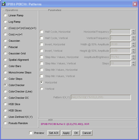
The Patterns draws various test patterns in the image. The Sequence Patterns does the same on each image of a sequence.
The Set sets image pixels to a specified value. The Sequence Set does the same on each image of a sequence.

The Arithmetic provides pixel arithmetic, such as adding a constant value or multiplying by a constant value. The Sequence Arithmetic does the same on each image of a sequence. The Src+Dst Arithmetic does the same with distinct source and destination images.
The Binning provides averaging or integrating pixel values in ''bins'' of a checkerboard. The Sequence Binning does the same on each image of a sequence. The Src+Dst Binning does the same with distinct source and destination images.
The Contrast Modification allows modifying the image's contrast. The Sequence Contrast Modification does the same on each image of a sequence. The Src+Dst Contrast Modification does the same with distinct source and destination images.
The Convolution allows convolving the image with user-defined kernels. The Sequence Convolution does the same on each image of a sequence. The Src+Dst Convolution does the same with distinct source and destination images.
The Correlation Map allows correlating, or matching, a kernel image over a larger image, resulting in a profile image whose intensity, at each location, varies in proportion to the degree of match at that location. The Sequence Correlation Map does the same on each image of a sequence. The Src+Dst Correlation Map does the same with distinct source and destination images.
The Edge Detection provides Kirsch, Sobel, and other standard edge detectors. The Sequence Edge Detection does the same on each image of a sequence. The Src+Dst Edge Detection does the same with distinct source and destination images.
The FFT provides Fast Fourier Transforms and Discrete Fourier Transforms. The Sequence FFT does the same on each image of a sequence. The Src+Dst FFT does the same with distinct source and destination images.
The HSB Tweak provides hue, saturation, and brightness adjustments within the HSB color space. While Arithmetic and other operations can optionally use the HSB color space to, for example, multiply all saturation values by a constant, the HSB Tweak allows adjusting selected portions of the HSB space, such as adjusting the brightness of red pixels with high saturation. The Sequence HSB Tweak does the same on each image of a sequence. The Src+Dst HSB Tweak does the same with distinct source and destination images.
The Interlace & Flicker provides line and pixel shuffling operations. The Sequence Interlace & Flicker does the same on each image of a sequence. The Src+Dst Interlace & Flicker does the same with distinct source and destination images.

The Morphology provides morphological operations with user-defined kernels. The Sequence Morphology does the same on each image of a sequence. The Src+Dst Morphology does the same with distinct source and destination images.
The Noise Generator allows adding pseudo-random noise with uniform and other distributions to an image. The Sequence Noise Generator does the same on each image of a sequence. The Src+Dst Noise Generator does the same with distinct source and destination images.
The Normalization provides intensity normalizations based upon a single image. The Sequence Normalization does the same on each image of a sequence. The Src+Dst Normalization does the same with distinct source and destination images.
The Rotation & Shift provides image rotations and shifts. The Sequence Rotation & Shift does the same on each image of a sequence. The Src+Dst Rotation & Shift does the same with distinct source and destination images.
The Spatial Filtering provides low pass, high pass, and other filters. The Sequence Spatial Filtering does the same on each image of a sequence. The Src+Dst Spatial Filtering does the same with distinct source and destination images.
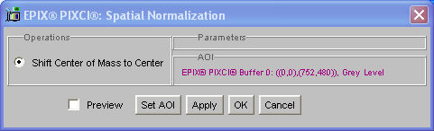
The Spatial Normalization provides spatial normalizations based upon a single image. The Sequence Spatial Normalization does the same on each image of a sequence. The Src+Dst Spatial Normalization does the same with distinct source and destination images.
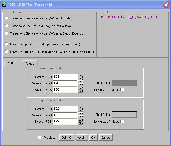
The Threshold allows thresholding an image against user-defined, fixed, boundary values. The Sequence Threshold does the same on each image of a sequence. The Src+Dst Threshold does the same with distinct source and destination images.

The Threshold Adaptive allows thresholding an image against boundary values that are automatically adjusted. The Sequence Threshold Adaptive does the same on each image of a sequence. The Src+Dst Threshold Adaptive does the same with distinct source and destination images.
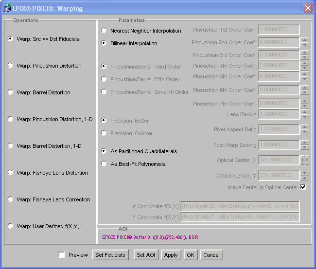
The Warping allows ''rubber-sheet'' transformations governed by a list of initial and final fiducial locations, governed by pincushion/barrel lens distortion, or specified by mathematical expressions. The Sequence Warping does the same on each image of a sequence. The Src+Dst Warping does the same with distinct source and destination images.
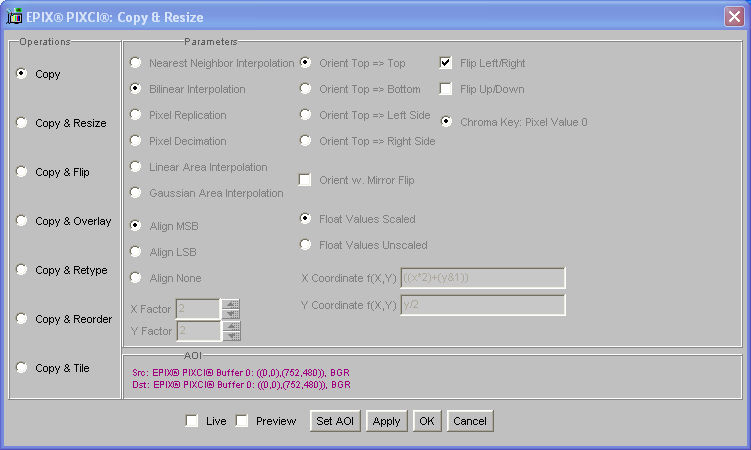
The Copy & Resize allows copying and resizing an image from one image buffer to another. The Sequence Copy & Resize does the same on each image of a sequence.

The Pair Arithmetic provides pixel arithmetic, such as summation, between one image buffer and another. The Src+Dst Arithmetic does the same with distinct source and destination images.
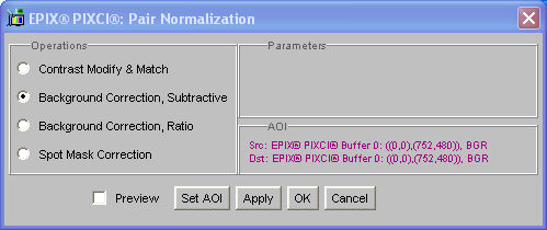
The Pair Normalization allows normalizing various intensity based attributes of an image, based upon a second reference, or background, image. The Src+Dst Pair Normalization does the same with distinct source and destination images.
The Triplet Normalization allows normalizing various intensity based attributes of an image, based upon two other reference, or background, images. The Src+Dst Triplet Normalization does the same with distinct source and destination images.
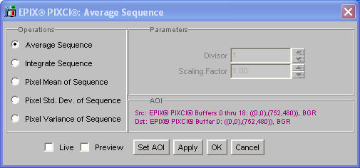
The Average Sequence allows forming the average or sum of an image sequence.
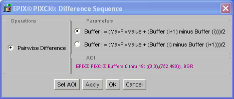
The Difference Sequence allows forming the difference of each pair of images of an image sequence.
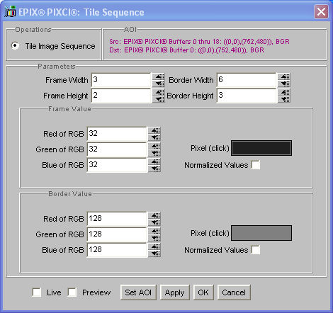
The Tile Sequence allows forming a grid of reduced images from an image sequence.
For image copy and other image processing operations utilizing a distinct source and destination, the image viewer window from which the operation is selected is always the modified destination; an image (or sequence) associated with a different image viewer window can be selected as the unmodified source.
5.2.5. Image Viewer - Measure
The image viewer window's Measure provides features for image measurement and analysis, including user-defined coordinate systems and mapping intensities into user-defined units.
The Intensity Calibration allows creating a mapping (correspondence) from monochrome image pixel values into user-defined units, for example from grey level into brightness, or grey level into density of material.
The Spatial Calibration allows creating a mapping (correspondence) from pixel X,Y coordinates into a user-defined H,V coordinate system. The H,V coordinates may be translated, scaled, and/or rotated with respect to X,Y coordinates.
The Histogram computes and displays a graph of an image's histogram.
The Histogram Pair computes and displays a graph of the histogram of difference of a pair of images.
The Mass & Moments computes and displays various moments of an image.
The Line Profile displays a two-dimensional graph of pixels values along an arbitrary oriented line, arc, polyline, Bezier, and other curves.
The Radial Mass Plot displays a two-dimensional graph of the sum of pixel values versus the pixels' distance from an origin.
The Ruler overlays a ruler on the image, with user-defined length, width, and tick marks, all based on the H,V coordinate system. Multiple rulers can be overlaid on each image.
The Protractor overlays a protractor on the image, with user-defined radius, arc, and tick marks, all based on the H,V coordinate system. Multiple protractors can be overlaid on each image.
The Cartesian Reticle overlays a Cartesian coordinate reticle on the image, based on the H,V coordinate system. Multiple Cartesian reticles can be overlaid on each image.
The Polar Reticle overlays a polar coordinate reticle on the image, based on the H,V coordinate system. Multiple polar reticles can be overlaid on each image.
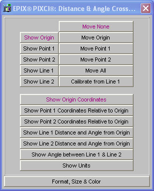
The Distance & Angle Crosshairs provides spatial calibration and measurement of absolute position, relative position, length and angles. While these capabilities are also available elsewhere in Image Viewer - Measure and Image Viewer - Draw, the Distance & Angle Crosshairs collects chosen features to provide a single window with the equivalent of a so-called ''Video Crosshair Overlay & Measurement'' system.
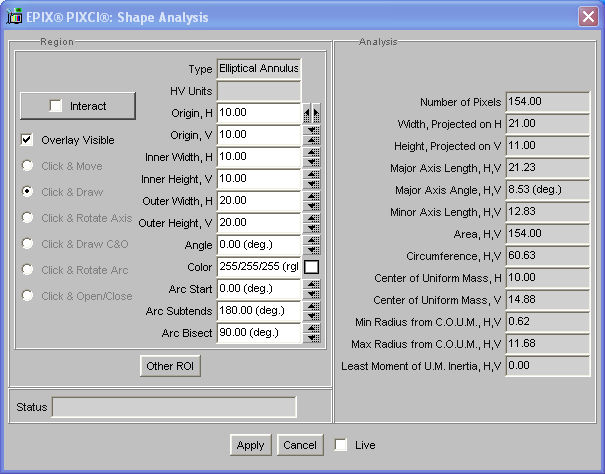
The Shape Analysis provides descriptive statistics about the shape of elliptical, rectangular, or polygonal regions.
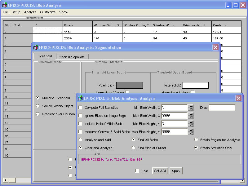
The Blob Analysis identifies image blobs, based upon thresholding the image into foreground and background, and provides descriptive statistics about the blobs found.
The Particle Tracking provides identification and tracking of particles (blobs) over a sequence of images. Individual particles are detected based upon a thresholded (bi-level) image. In one method, multiple image occurrences of a common particle are identified across a sequence of images by position extrapolation and verification. In a second method, vectors of particles that are close together are compared and expected to yield consistent magnitude and direction. In a third method, which requires the fewest setup parameters, common particles are grouped by nearest neighbor. For any method, the particle's trajectories are displayed and reported.
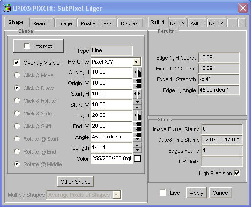
The SubPixel Edger overlays a line or curve tool on the image, analyzes the pixel values under the line or curve finding edges or lines to subpixel accuracy, and displays the position of the edges or lines both graphically, on the image, and numerically.
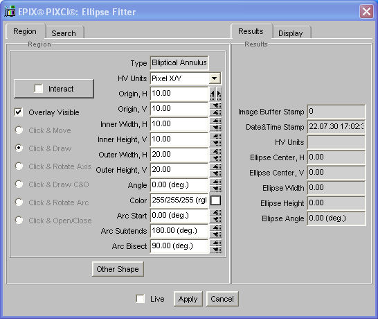
The Ellipse Fitter overlays an elliptical pattern of subpixel edger tools on the image, and computes a best-fit elliptical curve from the edges found.
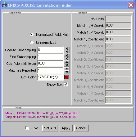
The Correlation Finder correlates, or matches, a kernel image over a larger image, showing the coordinates of, and displaying a box around, the best match(es).
5.2.6. Image Viewer - Draw
The image viewer window's Draw provides features for drawing graphics and text over the image. One or more of: line, circle with aspect ratio correction, rotated rectangle, rotated ellipse, arc of circle with aspect ratio correction, arc of rotated ellipse, annulus, arc of annulus, rectangular frame, list of points, polygon, polyline (connected line segments not closed into a polygon), Bezier curve, or Bezier region (Bezier curve closed to form region), rotated text, and arrow may be overlaid over the image (non destructive) or written into the image. The individual menu items such as Text, Line, Rectangle, etc. allow quick drawing of graphics or text. The Graphic Manager permits drawing the same graphics or text, but in addition manages a list of graphic or text objects, including loading and saving of the graphic or text objects.
The Image Overlay feature allows overlaying a second image, containing graphics on a ''transparent'' background, over the current image.
The Paint Brush feature allows interactive ''painting'' onto the image with selectable color, patterns, and ''brush'' shapes.
The Paint Fill feature allows filling (flooding) an image region with ''paint'' of selectable color and patterns, using specified pixel values as the boundary terminating the ''filling''.
5.2.7. Image Viewer - AOI
The image viewer window's Aoi allows defining areas of interest (AOI) and regions of interest (ROI) upon which future image processing, measurement, analysis, print, load, and save features will operate. As used in XCAP, an ''AOI'' is a rectangular area with sides parallel to the image axis, while an ''ROI'' is of arbitrary shape, such as an ellipse or rectangle which may be rotated with respect to the image axis, or an arbitrary path or polygon. The image print, load, save, and many other features only allow use of an AOI; selected image processing, measurement, analysis and other features also allow use of an ROI.
The Set AOI defines the default area of interest and color space upon which future image processing, printing, load, and save features will operate.
The Set ROI defines the default region of interest and color space upon which future image measurement, analysis, and other selected features which accept an ROI will operate.
The Set Full Image quickly sets the default area of interest and region of interest to the image's full dimensions, and the default color space to the image buffer's natural color space, without entering the Set AOI or Set ROI window.
The AOI/ROI Manager maintains a list of often used areas of interest (AOI) and regions of interest (ROI).
Within each of the image processing, measurement, analysis, print, load, and save features a different AOI (or ROI, if applicable) can be selected, temporarily overriding the default AOI (or ROI). Within the feature, the new AOI (or ROI) can be specified numerically or interactively drawn, or an AOI (ROI) previously defined within the AOI/ROI Manager can be selected.
5.2.8. Image Viewer - View - Shortcuts
A tool bar of icons provides shortcuts for accessing often used features of The Image Viewer Window. Selected shortcuts can also be activated by key clicks when the tool bar window has the ''input focus'' (i.e. that window's title bar is highlighted). The shortcuts provided are:
- Switch to first buffer of sequence (Key HOME).
- Switch to next buffer of sequence (Key PAGE UP).
- Switch to previous buffer of sequence (Key PAGE DOWN).
- Switch to last buffer of sequence (Key END).
- Copy image to new image buffer.
- Adjust palette.
- Activate or deactivate zoom (i.e. magnification).
- Peek at numeric pixel values.
- Activate or deactivate cursor overlay.
- Draw a two-dimensional plot of line or column of pixel values.
- Draw a histogram of pixel values.
- Select: (a) Resizing of the image to fit The Image Viewer Window with correct aspect ratio, (b) No resizing so that there is a one to one relationship between an image pixel and a graphics display system's pixel thereby avoiding resizing artifacts (although the entire image may not fit within the window and must therefore be panned and scrolled, and the displayed aspect ratio will be incorrect for images whose aspect ratio differs from the graphic display system's aspect ratio), or (c) Resize the image via pixel decimation or replication thereby avoiding resizing artifacts (although the displayed aspect ratio will be incorrect for images whose aspect ratio differs from the graphic display system's aspect ratio).
The shortcuts may either be attached and part of The Image Viewer Window, or may be detached into its own window, as set by Display under Image Viewer - View.
5.2.9. Image Viewer - View - Status Bar
A status bar provides information about the image resolution, current cursor coordinates, current buffer of a sequence, and other similar information. The information to be shown can be selected by Display under Image Viewer - View.
5.2.10. PIXCI® Image Viewer - Capture
The image viewer window associated with the PIXCI® frame grabber's image frame buffer(s) has Capture which provides for capturing images from the PIXCI® frame grabber and other features associated with the PIXCI® frame grabber. Any additional image viewer windows created by Launch 2nd Viewer do not provide Capture, but only view, modify, examine, and/or draw the frame buffers.
The Snap captures and displays a single image. The Live continuously captures and displays images; the UnLive terminates the Live mode, displaying the last captured image.
The First Buffer switches to the first buffer of the frame buffer sequence, the Last Buffer switches to the last buffer of the frame buffer sequence, the Next Buffer switches to the next buffer of the frame buffer sequence, and the Previous Buffer switches to the previous buffer of the frame buffer sequence.
The Adjustments allows setting common adjustments, as suitable for the model of the PIXCI® frame grabber in use. For the PIXCI® SV2, SV3, SV4, SV5, SV5A, SV5B, and SV5L models, the Adjustments allows selecting the video input connection (N/A for PIXCI® SV5B) and adjusting the gain, black level, hue, and saturation.
For the PIXCI® SV7 model, the Adjustments allows selecting AGC and adjusting the gain, black level, hue, and saturation.
For the PIXCI® SV8 model, the Adjustments allows selecting AGC and adjusting the gain, black level, hue, saturation, and sharpness.
For the PIXCI® A110 and A310 models, the Adjustments allows adjusting the analog gain and offset, and the digital gain and offset. Less frequently used, and more esoteric, adjustments may be found under PIXCI® Video Setup, described above. For the PIXCI® CL1, CL3SD, D, D24, D32, D2X, D3X, and D3XE models, the Adjustments provide camera specific controls.
For the PIXCI® CL2, E1, E1DB, E4, E4DB, E4G2-2F, E4G2-4B, E4G2-F2B, E4TX2-2F, E4TX2-4B, E4TX2-F2B, E8, E8DB, e104x4-2f, e104x4-4b, e104x4-f2b, EB1, EB1G2, EB1-PoCL, EB1G2-PoCL, EB1mini, miniH2B, miniH2F, miniH2x4F, mf2280, EC1, ECB1, ECB1-34, ECB2, EL1, and EL1DB models, the Adjustments provide camera specific controls. Or, for ''Generic Camera Link'' mode, the Adjustments allow configuring the PIXCI® frame grabber's video resolution, trigger modes, bit depth, color space, etc. so as to be consistent with the camera.
For the PIXCI® E8CAM, ELS2, SI, SI1, SI2, and SI4 models, the Adjustments provide camera specific controls.
The Adjustments also provide duplicate features to Snap, Live, UnLive, select the frame buffer, and set the video window size. A duplicate menu item to access Adjustments is provided under Image Viewer - View.
The Shortcuts activates or deactivates the PIXCI® Image Viewer - Capture - Shortcuts, described below. A duplicate menu item to access Shortcuts is provided under Image Viewer - View.
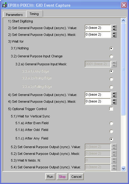
The GIO Event Capture provides single or sequence image capture, each image triggered in conjunction with the frame grabber's general purpose (formerly referred to as an external TTL) input and output signals.
The Sequence Capture features allow capturing a timed sequence of images. The Sequence Capture features may be started by an event (trigger), run continuously until stopped by an event, or each individual image may be captured in response to an event. Events include mouse clicks, time of day, and the frame grabber's general purpose (formerly referred to as external TTL) inputs; when used with general purpose input events the Sequence Capture differs from GIO Event Capture in that the latter provides more options and higher accuracy and repeatability for the manipulation of the general purpose inputs and outputs in response to video timing. A time stamp feature allows recording the time that each image was captured, and either overlaying the time nondestructively or permanently marking the image with the time.
A variety of Sequence Capture features provide tradeoffs between capture rate vs. convenience vs. total number of images captured.
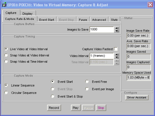
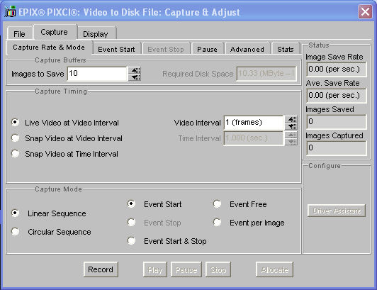
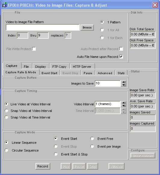
The Waterfall Display displays a chosen line of the frame buffer, in a ''waterfall'' fashion, updating the screen once per field, or as often as the host computer's speed allows. This feature is primarily intended for adjusting line scan type cameras. The waterfall display is intended only for viewing; it can't be analyzed, and can be saved only as a side effect of Screen Capture.
The Video to StreamStor (only under Windows) allows recording and playing video to and from Boulder Instruments StreamStor High-Speed Disk Recorders, allowing recording at video rate with almost all cameras and resolutions. The Video to StreamStor is provided only in the XCAP-Plus version.
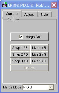
The RGB Merge allows interpreting and viewing three monochromatic frame buffers as a single color (e.g. RGB) image, with adjustments for registration and coloring.
The Quad Pixel Merge allows interpreting and viewing four monochromatic frame buffers, each one captured after shifting the image sensor by ½ pixel horizontally and vertically, as a single high resolution image.
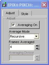
The Frame Average allows performing recursive, continuous, averaging of live video frames (or fields) and viewing the live result.
The Live Options combines the View - Display options, above, with additional choices governing Live mode. During Live mode, the PIXCI® frame grabber can: (a) Capture continuously into the specified frame buffer, however the image shown on the graphics display may contain portions from different video frames, (b) Snap, display on the graphics display, and repeat, however the image capture and display rate will be slower, or (c) Alternate capturing into the specified frame buffer and the last frame buffer (dual buffering). On host computers with insufficient PCI bandwidth to simultaneously capture into host computer memory and display from host computer memory to the graphics display, option (b) reduces the required bandwidth by approximately half.
The Lens Control - Birger EF232 allows controlling the aperture and focus of a compatible lens via a Birger EF232 Lens Mount. Both manual aperture and focus control, through the GUI, as well as automatic aperture and focus control, in response to the image intensity and sharpness, are provided.
5.2.11. PIXCI® Image Viewer - Capture - Shortcuts
A tool bar of icons provides shortcuts for accessing often used features of the PIXCI® frame grabber, and is an extension of the Image Viewer - View - Shortcuts described above. Selected shortcuts can also be activated by key clicks when the tool bar window has the ''input focus'' (i.e. that window's title bar is highlighted). The shortcuts provided are:
- Switch to first buffer of frame buffer sequence (Key HOME).
- Switch to next buffer of frame buffer sequence (Key PAGE UP).
- Switch to previous buffer of frame buffer sequence (Key PAGE DOWN).
- Switch to last buffer of frame buffer sequence (Key END).
- Snap single image (Key S).
- Toggle between:
- Duplicate image.
- Adjust palette.
- Activate or deactivate zoom (i.e. magnification).
- Activate or deactivate cursor overlay.
- Select: (a) Resizing of the image to fit The Image Viewer Window with correct aspect ratio, (b) No resizing so that there is a one to one relationship between an image pixel and a graphics display system's pixel thereby avoiding resizing artifacts (although the entire image may not fit within the window and must therefore be panned and scrolled, and the displayed aspect ratio will be incorrect for images whose aspect ratio differs from the graphic display system's aspect ratio), or (c) Resize the image via pixel decimation or replication thereby avoiding resizing artifacts (although the displayed aspect ratio will be incorrect for images whose aspect ratio differs from the graphic display system's aspect ratio).
- Peek at numeric pixel values.
- Draw a two-dimensional plot of line or column of pixel values.
- Draw a histogram of pixel values.
- Acquire sequence.
- Display sequence.
The shortcuts may either be attached and part of The Image Viewer Window, or may be detached into its own window, as set by Display under Image Viewer - View.
5.3. Other Features
Other useful features of XCAP are associated with many, or all, of its windows.
Most windows of XCAP provide fields for numeric entry. Typically, to the right of the numeric entry field are two up/down or left/right buttons. Left clicking a button allows incrementing or decrementing the numeric value. Left clicking within a button's shaded area yields larger increment or decrement values, depending on the distance from the opposite button.
Right clicking the numeric field, either button, or the area between buttons, yields an options menu. The options menu typically provides the following:
- Selecting the base to which integer numbers are displayed, or the format and precision to which non-integer numbers are displayed.
- Changing the increment and decrement values to be applied when the buttons are left clicked. Selecting whether the increment or decrement is added or subtracted, whether a percentage up or down, or is the number of ''steps'' unique to that numeric field.
- Activating a ScrollPad (a miniature scroll bar which overlays the displayed number) allowing adjustment of the numeric value with mouse clicks and drags.
- Selecting units and range for display of angles, such as 0 to 360 degrees, -180 degrees to +180 degrees, 0 to 2pi radians, or -pi to +pi radians.
- Selecting units for display of temporal intervals, such as milliseconds, seconds, minutes, or hours.
- Selecting units for display of lengths, such as millimeters, centimeters, meters, inches, or feet.
- Selecting units for display of frequencies, such as Hertz, kiloHertz, megaHertz, or the corresponding period in seconds, milliseconds, or microseconds.
- Selecting units for display of memory sizes, such as bytes, kilobytes, megabytes, gigabytes, or IEC kibibytes, IEC mebibyte, IEC gibibyte, etc.
- Selecting units for display of temperature, such as Fahrenheit, Celsius, or Kelvin.
- Connecting the field to receive new content from a specified cell of the Black Board, or connecting the field to transmit its content to a specified cell of the Black Board.
- Providing a larger Big Field in which to view or enter a number.
- Providing an Expression field in which a mathematical expression can be entered and evaluated to a numeric value.
- Providing editing controls such as Cut, Copy, Paste, and Delete.
Some numeric fields may have an associated, explicit, ''slider'' control in addition to the implicit ScrollPad. Right clicking the slider allows enlarging a portion of the slider's range for finer control.
Various windows of XCAP provide fields for entry of text, or file and path names. Right clicking the field yields an options menu. The options menu typically provides the following:
- Connecting the field to receive new content from a specified cell of the Black Board, or connecting the field to transmit its content to a specified cell of the Black Board.
- Providing a larger Big Field in which to view or enter text.
- Providing a history of previously used values, allowing convenient reuse without retyping.
- Providing editing controls such as Cut, Copy, Paste, and Delete.
- Automatically generating a unique file name representing the current date and time (for files to be saved or created).
Various windows of XCAP provide fields for entry of pixel colors. Typically, the color can be entered numerically, and a small color ''swatch'' appears next to the color entry field, showing the selected color. Right clicking the swatch activates a color cylinder from which new colors may be selected by mouse clicks.
Various windows of XCAP provide a drop-down list selection field. Right clicking the selection field yields an options menu which in turn provides a Search feature. The Search allows convenient searching through a long list of selections. Selected drop-down list selection fields may have an explicit, adjacent, Search button to access the same service.
For drop-down list selection fields used to select a serial ''COM'' port (for Windows) or ''ttyS'' device (for Linux), right clicking the selection field yields an options menu which in turn provides a Refresh feature which updates the list based on the operating system's currently installed ports or devices.
Editing of numeric and text fields follows standard conventions. In brief, mouse click once or use left/right arrow keys to position the caret - characters are inserted at the caret as typed. Double mouse click to highlight all text or single click and drag to highlight a portion of text - a Delete or Backspace removes the highlighted text, a character replaces the highlighted text, and the left/right arrow keys cancel the highlight mode.
Hovering the mouse over a numeric, text, list selection, checkbox, radio button, button, or other control will cause the associated Tool Tip, if any, to pop-up; the Tool Tip will automatically disappear. The Tool Tip can also be displayed by right-clicking on the control for its options menu, which in turn provides a Tool Tip feature; the Tool Tip must be explicitly closed. The Big Field, Expression, and Search features also display the Tool Tip.
The user interface can be navigated without a mouse by using Tab and Shift-Tab to shift input focus, arrow keys and PgUp/PgDn to scroll, arrow keys to select tabs and list items, Enter to select choices and push buttons, and Alt-Tab (under Windows) or Ctrl-Alt-Tab (under Linux) to select a Window.
5.4. Road Map - Main Window
Main Window

    File
        Load New Image
        Load New Image Sequence
            AVI
            BigTIFF
            BMP
            FITS
            JPEG/JFIF
            TIFF
            Portable Map
            VIF (Video Frame Files - Video to Disk)
            Multimedia
        Image File Info
        TWAIN Select Source
        TWAIN New Acquire
        TWAIN Source Info
        Window List
         -- List of current windows
        Exit

    Images
        New Image
        -- List of current images

    Scripts
        Script Record
        Script Play
        Script Remote Control
        Script Edit
        Script Tools
        Load Tool Bar
        Freeze Display
        Thaw & Refresh Display

    Utility
        Black Board
        Message Log
        Audio Clip (Windows only)
        RS-232 Terminal
        Screen Capture
        I/O Port Peek & Poke (Windows 95, 98, ME only)
        Program Setup
        Windows Info (Windows only)
        Linux Info (Linux only)
        Window Style
        Java Info
        Devices
            Birger EF232
            Directed Perception Pan-Tilt Unit
            EPIX® SILICON VIDEO® 10C-CL
            EPIX® SILICON VIDEO® 10M-CL
            EPIX® SILICON VIDEO® 20C-CL
            EPIX® SILICON VIDEO® 20M-CL
            EPIX® SILICON VIDEO® 1514CL
            EPIX® SILICON VIDEO® 1820CL
            Fujinon CCTV Lens
            Illumination Technologies 3900
            Sagebrush Pan-Tilt Gimbal
            Volpi intralux dc-1100

    PIXCI®
        PIXCI® Open/Close
            Multiple Devices
            Camera & Format
            Driver Assistant
            Advanced
            Board Info
        PIXCI® Video Setup
            Format  (dependent on frame grabber)
            Resolution
            Sync
            Custom

        PIXCI® Export Video Setup
        PIXCI® Import Video Setup
        PIXCI® TWAIN Sourcery (Windows only)
        PIXCI® Image-Pro Sourcery (Windows only)
        PIXCI® Status
        PIXCI® Serial Terminal
        PIXCI® Connections
        PIXCI® Camera Info

    Help
        About
        License
        XCAP Release Notes
        XCAP Reference Manual
        PCI Configuration Tips
        Getting Started w. XCAP (via Web)
            for PIXCI® A110
            for PIXCI® A310
            for PIXCI® CL1
                ...
            for SILICON VIDEO® 10M6
            for SILICON VIDEO® 10C6
                ...
5.5. Road Map - PIXCI® Image Viewer Window
PIXCI® Image Viewer Window

    File
        Save Image
            BigTIFF
            BMP
            FITS
            JPEG/JFIF
            Portable Map
            TIFF
            X/Y Binary
            X/Y ASCII

        Load Image
            TIFF
            BigTIFF
            JPEG/JFIF
            BMP
            FITS
            Portable Map
            X/Y Binary
            X/Y ASCII

        Save Image Sequence
            One AVI/DIB w. Sequence
            One AVI/MJPG w. Sequence
            One BigTIFF w. Sequence
            One FITS w. Sequence
            One Portable Map w. Sequence
            One TIFF w. Sequence
            One X/Y Binary w. Sequence
            One X/Y ASCII w. Sequence
            Sequence of BigTIFF
            Sequence of BMP
            Sequence of FITS
            Sequence of JPEG/JFIF
            Sequence of TIFF
            Sequence of Portable Map
            Sequence of X/Y Binary
            Sequence of X/Y ASCII

        Load Image Sequence
            One AVI w. Sequence
            One BigTIFF w. Sequence
            One FITS w. Sequence
            One TIFF w. Sequence
            One Portable Map w. Sequence
            One X/Y Binary w. Sequence
            One X/Y ASCII w. Sequence
            Sequence of BigTIFF
            Sequence of BMP
            Sequence of FITS
            Sequence of JPEG/JFIF
            Sequence of TIFF
            Sequence of Portable Map
            Sequence of X/Y Binary
            Sequence of X/Y ASCII

        E-Mail Image
        Save Frame Buffer Memory
        Load Frame Buffer Memory
        Print Image
        Duplicate Image
        Duplicate Image Sequence
        BlackBoard Image
        Image Attributes
        Close Viewer

    View
        Shortcuts
        Adjustments
        Status Bar
        Menu Bar
        Full Screen
        Always-On-Top
        Refresh
        Image's Palette
        Viewer's Palette
            Black & Gain
            Numerically
            Band Coloring
            Bit Slice
            Bit Transposition
            White Balance

        Sequence Play
        Sequence Thumbnails
        Cursor
        Display
        Zoom, Pan, Scroll
        Flip & Mirror
        Launch 2nd Viewer

    Examine
        Pixel Peek
            Peek X/Y
            Peek X/B
            Peek Y/B
        Pixel Peek & Poke
        Pixel Plot
            Plot Row
            Plot Column
            Plot Buffer
            Plot All Rows

        Pixel Plot 3D
        Pixel Magnifier
        SMPTE VITC

    Modify
        Patterns [Sequence Patterns]
        Set [Sequence Set]
        Arithmetic [Sequence Arithmetic] [Src+Dst Arithmetic]
            Complement Pixels
            Bit Wise Logical AND Pixels w. Mask
            Bit Wise Logical XOR Pixels w. Mask
            Bit Wise Logical OR Pixels w. Mask
            Bit Shift Left
            Bit Shift Right
            Bit Rotate Left
            Bit Rotate Right
            Bit Gray Code
            Bit Gray Decode
            Bit Reverse
            Add Constant with Pixels
            Multiply Constant with Pixels
            Add Uniform Random Dither to Pixels
            Add Gaussian Random Dither to Pixels
            Halftone, Threshold & Carry
            Halftone, Dot Construction
            Gamma Correction
            Pixie Minimum
            Pixie Maximum
            Pixie Mean
            Pixie Copy

        Binning [Sequence Binning] [Src_Dst Binning]
            Average
            Integrate

        Contrast Modification [Sequence Contrast Modification] [Src+Dst Contrast Modification]
            Stretch Contrast, Pixel Value Endpoints
            Stretch Contrast, Histogram Percentile Endpoints
            Invert Contrast
            Histogram Modification

        Convolution [Sequence Convolution] [Src+Dst Convolution]
            Convolve: Convolve(PixelValue)
            Convolve: Abs(Convolve(PixelValue))
            Convolve: PixelValue Convolve(PixelValue)
            Convolve: PixelValue Abs(Convolve(PixelValue))

        Correlation Map [Sequence Correlation Map] [Src+Dst Correlation Map]
        Edge Detection [Sequence Edge Detection] [Src+Dst Edge Detection]
            Edge Magnitude: Laplacian
            Edge Magnitude: Vertical
            Edge Magnitude: Horizontal
            Edge Magnitude: Sobel
            Edge Magnitude: Kirsch
            Edge Magnitude: Roberts
            Edge Gradient: Log Sobel
            Edge Gradient: Log Sobel Absolute
            Edge Gradient: Log Kirsch
            Edge Gradient: Log Roberts
            Edge Gradient: Thin, Minimal Effect
            Edge Gradient: Thin, Maximal Effect

        FFT [Sequence FFT] [Src+Dst FFT]
            FFT to Log Magnitude
            Root Filter
            Gaussian Filter
            Inverse Gaussian Filter

        HSB Tweak
        Interlace & Flicker [Sequence Interlace & Flicker] [Src+Dst Interlace & Flicker]
            Shuffle Line Order to Field Order
            Shuffle Field Order to Line Order
            Transpose Line Pairs
            Transpose Column Pairs
            Shuffle Line Pairs to Pixel Pairs
            Shuffle Pixel Pairs to Line Pairs
            Shuffle Column Order to Even-Odd Halves
            Shuffle Even-Odd Halves to Column Order
            Shuffle Column Order to N Section Order
            Shuffle N Section Order to Column Order
            Deflicker: Average Line Pairs
            Deflicker: Filter Singularity
            Shift Half-Line Down
            Shift Half-Line Up
            Tap Correction: User Defined f(X,Y)

        Morphology [Sequence Morphology] [Src+Dst Morphology]
            Erode
            Dilate
            Open
            Close
            Boundary
            Hit Miss
            Medial Axis Thin
            Skeleton Thin

        Noise Generator [Sequence Noise Generator] [Src+Dst Noise Generator]
            Uniform Noise
            Gaussian Noise
            Rayleigh Noise
            Negative Exponential Noise
            Salt & Pepper Noise

        Normalization [Sequence Normalization] [Src+Dst Normalization]
            Normalize Intensity, Blobs & Background
            Normalize Row Mean
            Normalize Column Mean

        Rotation & Shift [Sequence Rotation & Shift] [Src+Dst Rotation & Shift]
            X, Y Shift
            Flip
            Skew Left/Right
            Skew Up/Down
            Rotate
            Rotate w. Offset

        Spatial Filtering [Sequence Spatial Filtering] [Src+Dst Spatial Filtering]
            Low Pass Filter
            Sharpen Filter
            Median Filter
            Rank Low (Erode) Filter
            Rank High (Dilate) Filter
            Edge Enhance: Sobel
            Edge Enhance: Sobel Absolute
            Edge Enhance: Kirsch
            Edge Enhance: Roberts
            Horizontal Sharpen Filter
            Vertical Sharpen Filter
            Embossed Edges
            Emboss Enhance

        Spatial Normalization [Sequence Spatial Normalization] [Src+Dst Spatial Normalization]
            Shift Center of Mass to Center

        Threshold [Sequence Threshold] [Src+Dst Threshold]
        Threshold Adaptive [Sequence Threshold Adaptive] [Src+Dst Threshold Adaptive]
        Warping [Sequence Warping] [Src+Dst Warping]
            Warp: Src => Dst Fiducials
            Warp: Pincushion Distortion
            Warp: Barrel Distortion
            Warp: Pincushion Distortion, 1-D
            Warp: Barrel Distortion, 1-D
            Warp: Fisheye Lens Distortion
            Warp: Fisheye Lens Correction
            Warp: User Defined f(X,Y)
        Copy & Resize [Sequence Copy & Resize]
            Copy
            Copy & Resize
            Copy & Flip
            Copy & Overlay
            Copy & Retype
            Copy & Reorder
            Copy & Tile
        Pair Arithmetic [Sequence Pair Arithmetic] [Src+Dst Pair Arithmetic]
            Add: Dst+Src Modulo PixelSize
            Add: Min(Dst+Src, MaxPixValue)
            Subtract: (MaxPixValue+(Dst Src))/2
            Subtract: (MaxPixValue+(Src Dst))/2
            Subtract: (Dst Src)Modulo PixelSize
            Subtract: (Src Dst)Modulo PixelSize
            Subtract: (Src Dst)Modulo PixelSize
            Subtract: Max(Dst Src, 0)
            Subtract: Max(Src Dst, 0)
            Subtract: Abs(Dst Src)
            Bit Wise AND: Dst & Src
            Bit Wise XOR: Dst ^ Src
            Bit Wise OR: Dst | Src
            Average: (Src+Dst)/2
            Product: (c0*Src+c1)*(c2*Dst+c3)/c4
            Product: (c0*Dst+c1)/(c2*Src+c3)
            Ratio: (c0*Dst+c1)/(c2*Src+c3)
            User-Defined f(PixA, PixB)

        Pair Normalization [Sequence Pair Normalization] [Src+Dst Pair Normalization]
            Contrast Modify & Match
            Background Correction, Subtractive
            Background Correction, Ratio
            Spot Mask Correction

        Triplet Normalization [Sequence Triplet Normalization] [Src+Dst Triplet Normalization]
            Gain & Offset Normalization: MeanSrcB*(Dst-SrcA)/(SrcB-SrcA)
            Gain & Offset Normalization: MaxSrcB*(Dst-SrcA)/(SrcB-SrcA)
            Gain & Offset Normalization: MinSrcB*(Dst-SrcA)/(SrcB-SrcA)

        Average Sequence
            Average Sequence
            Integrate Sequence
            Pixel Mean of Sequence
            Pixel Std. Dev. of Sequence
            Pixel Variance of Sequence
        Difference Sequence
        Tile Sequence

    Measure
        Intensity Calibration
        Spatial Calibration
        Histogram
        Histogram Pair
        Mass & Moments
            Center of Mass
            Center of Mass, Binary
            Moments

        Line Profile
        Radial Mass Plot
        Ruler
        Protractor
        Cartesian Reticle
        Polar Reticle
        Distance & Angle Crosshairs
        Shape Analysis
        Blob Analysis
        Particle Tracking
        SubPixel Edger
        Ellipse Fitter
        Correlation Finder

    Draw
        Arrow
        Text
        Point
        Points
        Bezier Curve
        Circle
        Circle Arc
        Ellipse
        Ellipse Arc
        Line
        Parallel Lines
        Path Curve
        Polyline
        Rectangle
        Window
        Annulus
        Annulus Arc
        Bezier Region
        Elliptical Annulus
        Elliptical Annulus Arc
        Rectangle Array
        Path Enclosed
        Polygon
        Rectangular Frame
        Graphic Manager
        Image Overlay
        Paint Brush
        Paint Fill

    AOI
        Set AOI
        Set ROI
        Set Full Image
        AOI/ROI Manager

    Capture
        Adjustments
        Shortcuts
        Snap
        Live
        UnLive
        First Buffer
        Last Buffer
        Next Buffer
        Previous Buffer
        Sequence Capture
            Video to Frame Buffers - Single Sequence
            Video to Frame Buffers - Single Sequence w. Event Start
            Video to Frame Buffers - Single Sequence w. Event per Image
            Video to Frame Buffers - Continuous Sequence
            Video to Frame Buffers - Continuous Sequence w. Event Stop
            Video to Frame Buffers - Continuous Sequence w. Event per Image
            Video to Virtual Memory - Single Sequence
            Video to Virtual Memory - Single Sequence w. Event Start
            Video to Virtual Memory - Single Sequence w. Event per Image
            Video to Virtual Memory - Continuous Sequence
            Video to Virtual Memory - Continuous Sequence w. Event Stop
            Video to Virtual Memory - Continuous Sequence w. Event per Image
            Video to Disk File - Single Sequence
            Video to Disk File - Single Sequence w. Event Start
            Video to Disk File - Single Sequence w. Event per Image
            Video to Disk File - Continuous Sequence
            Video to Disk File - Continuous Sequence w. Event Stop
            Video to Disk File - Continuous Sequence w. Event per Image
            Video to Image Files - Single Sequence
            Video to Image Files - Single Sequence w. Event Start
            Video to Image Files - Single Sequence w. Event per Image
            Video to Image Files - Continuous Sequence
            Video to Image Files - Continuous Sequence w. Event Stop
            Video to Image Files - Continuous Sequence w. Event per Image
            Video to StreamStor (Windows only)
        GIO Event Capture

        Waterfall Display
        Video to Disk
        RGB Merge
        Quad Pixel Merge
        Frame Average
        Lens Control
            Birger EF232
        Live Options

    Help
        Vis-a-Vis
        PIXCI® --- User's Manual (via Web)
            (for specific PIXCIXCAP in use)
        SILICON VIDEO® --- User's Manual (via Web)
            (for specific SILICON VIDEOXCAP in use, if any)
Optionally, the Main Window and the PIXCI® Image Viewer Window's may be combined (see Utilities - Program Setup) with the following features of the Main Window added to the PIXCI® Image Viewer Window:
    File
        Window List
         -- List of current windows
        Image List
        -- List of current images
        Exit
    Utility
        Message Log
        Program Setup
        Windows Info (Windows only)
        Linux Info (Linux only)
        Window Style
        Java Info

    PIXCI®
        PIXCI® Open/Close
        PIXCI® TWAIN Sourcery (Windows only)
        PIXCI® Image-Pro Sourcery (Windows only)
        PIXCI® Connections
        PIXCI® Video Setup
        PIXCI® Serial Terminal

    Help
        XCAP Release Notes
        XCAP Reference Manual
        PCI Configuration Tips
        License
        About
Optionally, if XCAP is intended to be used solely in conjunction with a TWAIN compliant application or with Image-Pro, many of the menu features of the Main Window and the PIXCI® Image Viewer Window may be removed so as to provide a simplified appearance (see Utilities - Program Setup). The same option also removes several PIXCI® Image Viewer - Capture - Shortcuts and adds shortcuts duplicating features of the PIXCI® - TWAIN Sourcery and Image-Pro Sourcery.
5.6. XCAP Software Feature Comparison
| Feature | XCAP-Plus | XCAP-Std | XCAP-Ltd | XCAP-Lite | XCAP-Viewer |
| (A) | (A) | (A) | (A) | (A) | |
|
|
|||||
| File - | |||||
| - Load New Image | Yes | Yes | Yes | Yes (C) | Yes (C) |
| - Load New Image Sequence | Yes | Yes | Yes | Yes (C) | Yes (C) |
| - Image File Info | Yes | Yes | Yes | Yes | Yes |
| - TWAIN Select Source (Win) | Yes | Yes | No | No | No |
| - TWAIN New Acquire (Win) | Yes | Yes | No | No | No |
|
|
|||||
| Images - | |||||
| - New Image (Workspace) | Yes | Yes | Yes | Yes | Yes |
|
|
|||||
| Scripts - | |||||
| - Record | Yes | Yes | No | No | No |
| - Play | Yes | Yes | Yes | Yes | No |
| - Remote Control | Yes | Yes | No | No | No |
| - Load Tool Bar | Yes | Yes | No | No | No |
|
|
|||||
| Utility - | |||||
| - Black Board | Yes | Yes | No | No | No |
| - Message Log | Yes | Yes | Yes | Yes | Yes |
| - Audio Clip (Win) | Yes | Yes | Yes | Yes | No |
| - RS-232 Terminal | Yes | Yes | Yes | Yes | Yes |
| - Screen Capture | Yes | Yes | Yes | No | No |
| - I/O Port Peek & Poke (W95) | Yes | Yes | Yes | Yes | Yes |
| Devices - | |||||
| - Birger EF232 | Yes | Yes | Yes | Yes | Yes |
| - Directed Perception Pan-Tilt Unit | Yes | Yes | Yes | Yes | Yes |
| - EPIX® SILICON VIDEO® 10C-CL | Yes | Yes | Yes | Yes | Yes |
| - EPIX® SILICON VIDEO® 10M-CL | Yes | Yes | Yes | Yes | Yes |
| - EPIX® SILICON VIDEO® 20C-CL | Yes | Yes | Yes | Yes | Yes |
| - EPIX® SILICON VIDEO® 20M-CL | Yes | Yes | Yes | Yes | Yes |
| - EPIX® SILICON VIDEO® 1514CL | Yes | Yes | Yes | Yes | Yes |
| - EPIX® SILICON VIDEO® 1820CL | Yes | Yes | Yes | Yes | Yes |
| - Fujinon CCTV Lens | Yes | Yes | Yes | Yes | Yes |
| - Illumination Technologies 3900 | Yes | Yes | Yes | Yes | Yes |
| - Sagebrush Pan-Tilt Gimbal | Yes | Yes | Yes | Yes | Yes |
| - Volpi intralux dc-1100 | Yes | Yes | Yes | Yes | Yes |
|
|
|||||
| PIXCI® - | |||||
| - Open/Close - | |||||
| - Single Board | Yes | Yes | Yes | Yes | No |
| - Multiple Identical Boards | Yes | Yes | Yes | Yes | No |
| - Multiple Different Boards | Yes | Yes | No | No | No |
| - Frame Buffer Memory Limit - | |||||
| w. PIXCI® CL3SD | None (E) | None (E) | None (E) | None | N/A |
| w. PCI 32 bit | None (E) | None (E) | 4 GiByte (E) | 256 MiByte(E) | N/A |
| w. PCI 64 bit | None (E) | None (E) | 4 GiByte (E) | 256 MiByte(E) | N/A |
| w. PCI Express & 32 bit O.S. | None (E) | None (E) | 4 GiByte (E) | 256 MiByte(E) | N/A |
| w. PCI Express & 64 bit O.S. | None (E) | None (E) | 8 GiByte (E) | 256 MiByte(E) | N/A |
| w. ExpressCard/54 & 32 bit O.S. | None (E) | None (E) | 4 GiByte (E) | 256 MiByte(E) | N/A |
| w. ExpressCard/54 & 64 bit O.S. | None (E) | None (E) | 8 GiByte (E) | 256 MiByte(E) | N/A |
| w. mini PCIe & 32 bit O.S. | None (E) | None (E) | 4 GiByte (E) | 256 MiByte(E) | N/A |
| w. mini PCIe & 64 bit O.S. | None (E) | None (E) | 8 GiByte (E) | 256 MiByte(E) | N/A |
| w. M.2 & 32 bit O.S. | None (E) | None (E) | 4 GiByte (E) | 256 MiByte(E) | N/A |
| w. M.2 & 64 bit O.S. | None (E) | None (E) | 8 GiByte (E) | 256 MiByte(E) | N/A |
| - Driver Assistant/Wizard | Yes | Yes | Yes | Yes | No |
| - Video Setup | Yes | Yes | Yes | Yes | No |
| - Export Video Setup | Yes | Yes | Yes | Yes | No |
| - Import Video Setup | Yes | Yes | Yes | Yes | No |
| - TWAIN Sourcery (Win) | Yes | Yes | Yes | Yes | No |
| - Image-Pro Sourcery (Win) | Yes | Yes | Yes | Yes | No |
| - Status | Yes | Yes | Yes | Yes | No |
| - Serial Terminal | Yes | Yes | Yes | Yes | No |
| - Connections Info | Yes | Yes | Yes | Yes | Yes |
| - Camera Info | Yes | Yes | Yes | Yes | Yes |
| - Camera Specific Controls | Yes (F) | Yes (F) | Yes (F) | Yes (F) | No |
|
|
|||||
| Help - | |||||
| - XCAP Release Notes | Yes | Yes | Yes | Yes | Yes |
| - XCAP Reference Manual | Yes | Yes | Yes | Yes | Yes |
| - PCI Configuration Tips | Yes | Yes | Yes | Yes | Yes |
| - Getting Started w. XCAP (via Web) | Yes | Yes | Yes | Yes | Yes |
|
|
|||||
| File - | |||||
| - Save Image | Yes | Yes | Yes | Yes (C) | No |
| - Load Image | Yes | Yes | Yes | Yes (C) | Yes (C) |
| - Save Image Sequence | Yes | Yes | Yes | Yes (C) | No |
| - Load Image Sequence | Yes | Yes | Yes | Yes (C) | Yes (C) |
| - E-Mail Image | Yes | Yes | Yes | No | No |
| - Print Image | Yes | Yes | Yes | Yes (R) | No |
| - Duplicate Image | Yes | Yes | Yes | No | No |
| - Duplicate Image Sequence | Yes | Yes | Yes | No | No |
| - BlackBoard Image | Yes | Yes | No | No | No |
|
|
|||||
| View - | |||||
| - Full Screen | Yes (W) | Yes (W) | Yes (W) | Yes (W) | Yes (W) |
| - Frame-Less Full Screen | Yes (W) | Yes (W) | Yes (W) | No | No |
| - Palette | Yes | Yes | Yes | Yes (G) | Yes (G) |
| - Sequence Play | Yes | Yes | Yes | Yes | Yes |
| - Sequence Thumbnails | Yes | Yes | Yes | No | No |
| - Cursor | Yes | Yes | Yes | Yes | Yes |
| - Zoom, Pan, Scroll | Yes | Yes | Yes | Yes | Yes |
| - Flip & Mirror | Yes | Yes | Yes | Yes | Yes |
| - Multi-thread/CPU rendering | Yes | Yes | Yes | No | No |
| - Launch 2nd Viewer | Yes | Yes | Yes | No | No |
|
|
|||||
| Examine - | |||||
| - Pixel Peek X vs Y | Yes | Yes | Yes | Yes | Yes (H) |
| - Pixel Peek X vs B | Yes | Yes | Yes | Yes | Yes (H) |
| - Pixel Peek B vs Y | Yes | Yes | Yes | Yes | Yes (H) |
| - Pixel Peek & Poke | Yes | Yes | Yes | Yes | Yes |
| - Pixel Plot Row | Yes | Yes | Yes | Yes (I)(Y) | Yes (I)(Y) |
| - Pixel Plot Column | Yes | Yes | Yes | Yes (I)(Y) | Yes (I)(Y) |
| - Pixel Plot Pixel × B | Yes | Yes | Yes | Yes (I)(Y) | Yes (I)(Y) |
| - Pixel Plot Rows × Y | Yes | Yes | Yes | No | No |
| - Pixel Plot Rows × B | Yes | Yes | Yes | No | No |
| - Pixel Plot Cols × X | Yes | Yes | Yes | No | No |
| - Pixel Plot Cols × B | Yes | Yes | Yes | No | No |
| - Pixel Plot 3D | Yes | Yes | Yes | Yes (S) | Yes (S) |
| - Pixel Magnifier | Yes | Yes | Yes (Z) | No | No |
| - SMPTE VITC | Yes | Yes | Yes | No | No |
|
|
|||||
| Modify - | |||||
| - Patterns | Yes | Yes | Yes | Yes | Yes |
| - Set | Yes | Yes | Yes (J) | Yes (J) | Yes (J) |
| - Arithmetic | Yes | Yes | No | No | No |
| - Binning | Yes | Yes | No | No | No |
| - Contrast Modification | Yes | Yes | No | No | No |
| - Convolution | Yes | Yes | No | No | No |
| - Correlation Map | Yes | Yes | No | No | No |
| - Edge Detection | Yes | Yes | No | No | No |
| - FFT | Yes | Yes | No | No | No |
| - HSB Tweak | Yes | Yes | No | No | No |
| - Interlace & Flicker | Yes | Yes | No | No | No |
| - Morphology | Yes | Yes | No | No | No |
| - Noise Generator | Yes | Yes | No | No | No |
| - Normalization | Yes | Yes | No | No | No |
| - Rotation & Shift | Yes | Yes | No | No | No |
| - Spatial Filtering | Yes | Yes | No | No | No |
| - Spatial Normalization | Yes | Yes | No | No | No |
| - Threshold | Yes | Yes | No | No | No |
| - Threshold Adaptive | Yes | Yes | No | No | No |
| - Warping | Yes | Yes | No | No | No |
| - Copy & Resize | Yes | Yes | No | No | No |
| - Pair Arithmetic | Yes | Yes | No | No | No |
| - Pair Normalization | Yes | Yes | No | No | No |
| - Triplet Normalization | Yes | Yes | No | No | No |
| - Average Sequence | Yes | Yes | No | No | No |
| - Difference Sequence | Yes | Yes | No | No | No |
| - Tile Sequence | Yes | Yes | No | No | No |
|
|
|||||
| Measure - | |||||
| - Intensity Calibration | Yes | Yes | No | No | No |
| - Spatial Calibration | Yes | Yes | No | No | No |
| - Histogram | Yes | Yes | No | No | No |
| - Histogram Pair | Yes | Yes | No | No | No |
| - Mass & Moments | Yes | Yes | No | No | No |
| - Line Profile | Yes | Yes | Yes (K,L) | Yes (I,K,L) | Yes (I,K,L) |
| - Radial Mass Plot | Yes | Yes | No | No | No |
| - Ruler | Yes | Yes | Yes (K) | Yes (K) | Yes (K) |
| - Protractor | Yes | Yes | No | No | No |
| - Cartesian Reticle | Yes | Yes | Yes (K) | Yes (K) | Yes (K) |
| - Polar Reticle | Yes | Yes | No | No | No |
| - Dist. & Angle Crosshairs | Yes | Yes | No | No | No |
| - Shape Analysis | Yes | Yes | No | No | No |
| - Blob Analysis | Yes | Yes | No | No | No |
| - Particle Tracking | Yes | Yes | No | No | No |
| - SubPixel Edger | Yes | Yes | No | No | No |
| - Ellipse Fitter | Yes | Yes | No | No | No |
| - Correlation Finder | Yes | Yes | No | No | No |
|
|
|||||
| Draw - | |||||
| - Arrow | Yes | Yes | Yes | Yes | Yes |
| - Text | Yes | Yes | Yes | No | No |
| - Point | Yes | Yes | Yes | No | No |
| - Points | Yes | Yes | Yes | No | No |
| - Bezier Curve | Yes | Yes | Yes | No | No |
| - Circle | Yes | Yes | Yes | No | No |
| - Circle Arc | Yes | Yes | Yes | No | No |
| - Diamond | Yes | Yes | Yes | No | No |
| - Ellipse | Yes | Yes | Yes | No | No |
| - Ellipse Arc | Yes | Yes | Yes | No | No |
| - Line | Yes | Yes | Yes | Yes | Yes |
| - Parallel Lines | Yes | Yes | Yes | No | No |
| - Path Curve | Yes | Yes | Yes | No | No |
| - Polyline | Yes | Yes | Yes | No | No |
| - Rectangle | Yes | Yes | Yes | No | No |
| - Window | Yes | Yes | Yes | Yes | Yes |
| - Annulus | Yes | Yes | Yes | No | No |
| - Annulus Arc | Yes | Yes | Yes | No | No |
| - Bezier Region | Yes | Yes | Yes | No | No |
| - Elliptical Annulus | Yes | Yes | Yes | No | No |
| - Elliptical Annulus Arc | Yes | Yes | Yes | No | No |
| - Rectangle Array | Yes | Yes | Yes | No | No |
| - Path Enclosed | Yes | Yes | Yes | No | No |
| - Polygon | Yes | Yes | Yes | No | No |
| - Rectangular Frame | Yes | Yes | Yes | No | No |
| - Graphic Manager | Yes | Yes | Yes (B) | Yes (B) | Yes (B) |
| - Paint Brush | Yes | Yes | Yes | No | No |
| - Paint Fill | Yes | Yes | Yes | No | No |
| - Image Overlay | Yes | Yes | No | No | No |
|
|
|||||
| Capture - | |||||
| - Snap (Video) | Yes | Yes | Yes | Yes | No |
| - Live (Video) | Yes | Yes | Yes | Yes | No |
| - Frame Date&Time Stamp | Yes | Yes | Yes | Yes | No |
| - First Buffer | Yes | Yes | Yes | Yes | No |
| - Next Buffer | Yes (M) | Yes (M) | Yes (M) | Yes (M) | No |
| - Previous Buffer | Yes (M) | Yes (M) | Yes (M) | Yes (M) | No |
| - Last Buffer | Yes (M) | Yes (M) | Yes (M) | Yes (M) | No |
| - Adjustments - | |||||
| - Snap/Live Buffer Number | Yes | Yes | Yes | Yes | No |
| - Resolution (video window) | Yes | Yes | Yes | Yes | No |
| - Camera Specific Controls | Yes (F) | Yes (F) | Yes (F) | Yes (F) | No |
| - Color & White Balance | Yes (N) | Yes (N) | Yes (N) | Yes (N) | No |
| - SILICON VIDEO(R) AWB | Yes (N) | Yes (N) | Yes (N) | Yes (N) | No |
| - Auto Gain/Exposure Control | Yes (O) | Yes (O) | Yes (O) | No (O) | No |
| - SILICON VIDEO(R) AGC/AEC | Yes (O) | Yes (O) | Yes (O) | Yes (O) | No |
| - Pixel Normalization (FFC) | Yes (V) | Yes (V) | Yes (V) | Yes (V) | No |
| - Auto Contrast Enhancement | Yes (X) | Yes (X) | Yes (X) | No (X) | No | |
| - Manual Contrast Enhancement | Yes (X) | Yes (X) | Yes (X) | Yes (X) | No | |
| - Load & Save Presets | Yes | Yes | Yes | No | No |
| - Shortcuts | Yes | Yes | Yes | Yes | No |
| - GIO Event Capture Single | Yes | Yes | Yes | Yes | No |
| - GIO Event Capture Sequence | Yes | Yes | Yes | No | No |
| - Waterfall Display | Yes | Yes | Yes | Yes | No |
| - RGB Merge | Yes | Yes | Yes | No | No |
| - Frame Average | Yes | Yes | No | No | No |
| - Quad Pixel Merge | Yes | Yes | No | No | No |
| - Lens Control - | |||||
| - Birger EF232 | Yes | Yes | Yes(U) | Yes(U) | No |
|
|
|||||
| Sequence Capture (Single Sequence and Continuous Sequence) - | |||||
| - to Frame Buffers | Yes (E) | Yes (E) | Yes (E) | Yes (P)(E) | No |
| - to Frame Buffers at Event | Yes | Yes | Yes | No (Q) | No |
| - to Virtual Memory | Yes | Yes | Yes (T) | Yes (P)(T) | No |
| - to Virtual Memory at Event | Yes | Yes | Yes (T) | No (Q) | No |
| - to Image Files | Yes | Yes | Yes | Yes (D) | No |
| - to Image Files at Event | Yes | Yes | Yes | No | No |
| - to Image Files - FTP Copy | Yes | Yes | Yes | No | No |
| - to Image Files - HTTP Server | Yes | Yes | Yes | No | No |
| - to Disk File | Yes | Yes | No | No | No |
| - to Disk File at Event | Yes | Yes | No | No | No |
| - to StreamStor (Win) | Yes | No | No | No | No |
Notes: (A) For XCAP-Lite, the PIXCI® frame grabber is
assumed installed and open for use, otherwise XCAP-Lite provides
the same features as XCAP-Viewer. Use of XCAP-Plus, XCAP-Std, or
XCAP-Ltd with missing authorization key provides the same features
as XCAP-Lite. Use of XCAP without activation code, or never having
been configured for an authorization key, provides the features of
XCAP-Viewer.
(B) The Save, Import, and Export Graphic features are not
available in XCAP-Viewer, XCAP-Lite, or XCAP-Ltd.
(C) For XCAP-Viewer, images may not be saved; images may not
be loaded directly from an Internet URL. For XCAP-Lite, Save Image
Sequence is only available in TIFF format; images may not be loaded
directly from, or saved to, an Internet URL; and does not support
image ''stack'' options.
(D) For XCAP-Lite, the Sequence Capture to Image Files only
supports TIFF format.
(E) The maximum amount of frame buffer memory is dependent on
a the characteristics of the PIXCI® imaging card, the operating
system, and of XCAP software. The PIXCI® CL3SD and SI2 have
on-board frame buffer memory, other PIXCI® imaging cards use
computer based frame buffer memory. The PIXCI® CL1, CL2, D,
D24, D32, D2X, D3X, SI, SV2, SV3, SV4, and SV5 are designed to
access up to 4 GB of computer memory. The PIXCI® A110,
A310, D3XE, E1, E1DB, E4, E4DB, E4G2-2F, E4G2-4B, E4G2-F2B,
E4TX2-2F, E4TX2-4B, E4TX2-F2B, E8, E8CAM, E8DB, e104x4-2f,
e104x4-4b, e104x4-f2b, EB1, EB1G2, EB1-PoCL, EB1G2-PoCL, EB1mini,
miniH2B, miniH2F, miniH2x4F, mf2280, EC1, ECB1, ECB1-34, ECB2, EL1,
EL1DB, ELS2, SI1, SI4, SV7, and SV8 are designed to access up to
16 EiByte of computer memory (a theoretical limit, as no
currently available computer system provides 16 EiByte of
memory). For XCAP-Lite, a maximum of 256 MiByte of computer
based frame buffer memory is supported (but allows one full
resolution image buffer w/out size restriction). On 32 bit systems,
XCAP-Plus, XCAP-Std, and XCAP-Ltd support up to 4 GiBytes of
computer based frame buffer memory. On 64 bit systems, XCAP-Plus
and XCAP-Std supports up to 16 EiByte of computer based frame
buffer memory; XCAP-Ltd supports up to 8 GiByte of computer
based frame buffer memory. The maximum available computer based
frame buffer memory is also limited by the computer hardware,
configuration, and memory used by the operating system and other
applications.
(F) Camera specific controls provided for cameras supported by
PIXCI® E8CAM, ELS2, SI, SI1, SI2, and SI4, and for many digital
cameras supported by PIXCI® CL1, CL2, CL3SD, D, D24, D32, D2X,
D3X, D3XE, E1, E1DB, E4, E4DB, E4G2-2F, E4G2-4B, E4G2-F2B,
E4TX2-2F, E4TX2-4B, E4TX2-F2B, E8, E8DB, e104x4-2f, e104x4-4b,
e104x4-f2b, EB1, EB1G2, EB1-PoCL, EB1G2-PoCL, EB1mini, miniH2B,
miniH2F, miniH2x4F, mf2280, EC1, ECB1, ECB1-34, ECB2, EL1, and
EL1DB; the 'PIXCI® Camera Info' feature shows the specific,
customized, support provided for each camera.
(G) For XCAP-Lite and XCAP-Viewer, the Palette feature does
not include save, load, import, or export, nor the ''Extract
Bright/Dark Reference'' features.
(H) The Save Data feature is not available in XCAP-Viewer.
(I) For XCAP-Lite and XCAP-Viewer, the Pixel Plot feature does
not include statistics, save, export, or multi-image ''stack'' or
''plank'' options. For XCAP-Viewer, the Pixel Plot feature does not
include printing.
(J) For XCAP-Ltd, XCAP-Lite, and XCAP-Viewer, the Modify, Set
feature does not include non-rectangular regions.
(K) For XCAP-Ltd, XCAP-Lite, and XCAP-Viewer, the Measure
features do not include calibration.
(L) For XCAP-Ltd, XCAP-Lite, and XCAP-Viewer, the Line Profile
is limited to straight lines.
(M) Subject to the amount of frame buffer memory versus image
resolution yielding more than one frame buffer.
(N) Software implemented White Balance and Color Corrections
(in contrast to a camera's feature) is provided for SILICON
VIDEO® and other selected cameras; XCAP-Lite provides
automatic, continuous, white balance (AWB) only for SILICON
VIDEO® cameras. The XCAP-Lite does not provide custom color
calibration from a Macbeth chart or other color reference.
(O) Software implemented AGC/AEC (in contrast to a camera's
feature) is provided for selected cameras; of those, XCAP-Lite
provides AGC/AEC only for SILICON VIDEO® cameras.
(P) For XCAP-Lite, the Sequence Capture does not include the
graphic overlay of time stamp features, nor the strobe features
added by software (as selected in the Sequence Capture dialog); any
strobe features provided by the PIXCI® frame grabber or camera
(either inherent or selected in the Capture & Adjust dialog)
are available.
(Q) For XCAP-Lite, ''triggered'' sequence capture is provided
when the camera is, itself, triggered (often referred to as ''Async
Reset Mode''); sequence capture from a free-running camera where
the trigger or event is handled separately is not provided.
(R) For XCAP-Lite, the image printing feature only supports
use of the operating system's image printing feature(s), not
printing via EPIX® imaging drivers.
(S) The Save Graphics, Save Data, Export Data, or multi-image
''stack'' features are not available in XCAP-Viewer or XCAP-Lite.
The Print feature is not available in XCAP-Viewer.
(T) For XCAP-Lite, the sequence capture to virtual memory is
limited to using 1 GiByte of virtual memory For XCAP-Ltd, the
sequence capture to virtual memory is limited to using
4 GiByte of virtual memory. The operating system's
configuration may impose additional limitations.
(U) Interactive control of the lens is provided, but not
automatic aperture or automatic focus features in XCAP-Viewer or
XCAP-Lite.
(V) Software implemented Pixel Normalization or Flat Field
Correction (in contrast to a camera's feature) is provided for
SILICON VIDEO® and other selected cameras; of those, XCAP-Lite
does not provide Pixel Normalization in generic Camera Link
mode.
(W) Frame-less full screen is not available in XCAP-Lite,
XCAP-Viewer, or under Linux.
(X) Software implemented Contrast Enhancement (in contrast to
a camera's feature) is provided for selected cameras; of those,
XCAP-Lite provides manual, but not automatic contrast
enhancement.
(Y) The Save Graphics, Save Data, Copy Data, and Descriptive
Statistics features are not available in XCAP-Viewer or
XCAP-Lite.
(Z) The Contrast and other enhancements of the magnified area
not available in XCAP-Ltd.
(W95) Feature available only under Windows 95, 98, and ME.
(Win) Feature available only under Windows.
6. Getting Started with XCLIB
The optional XCLIB C/C++ library allows controlling the PIXCI® frame grabber from ''C/C++'' programs. Under Windows, the XCLIB library can also be accessed by any programming environment able to call functions within a DLL; such as VB.NET, C#, LabView, Matlab, and Python. Under Linux, the XCLIB library can also be accessed by any programming environment able to call functions within a Shared Object (SO); such as LabView, Matlab, and Python.
The XCLIB library is designed to be a component which is called by the user's application, rather than an application template with pre-selected and limited customizability. In other words, the XCLIB library forces the fewest possible architectural choices upon the user's application. Under Windows the XCLIB library is composed of ''C'' functions within a DLL and can be used from non-MFC, MFC, C#, or even ''console'' applications. With one optional exception, the XCLIB library does not create any windows or dialogs of its own; rather it allows displaying imagery into a window provided by the user.
This quick introduction focuses primarily on XCLIB library functions themselves; programming environment, operating system issues, and compilation instructions are addressed in the XCLIB Reference Manual and in the example programs provided with the XCLIB library. Nor is this introduction intended to cover every XCLIB library function or to provide complete programs; rather it is intended to provide the ''feel'' of XCLIB library programming, without the complications of user interfaces and application specific functionality.
Alternatives to use of XCLIB are available. The Media Foundation
Frame Server (DirectShow) driver for PIXCI® frame grabbers
provides a Windows Media Foundation, Media Source driver to control
PIXCI® frame grabbers and retrieve video and image data. The
Video for Linux Driver (V4L2) for PIXCI® frame grabbers
provides a Linux standard V4L2 API to control PIXCI® frame
grabbers and retrieve video and image data.
6.1. XCLIB Architecture Overview
The XCLIB library has two series of functions. The Simple C Functions (SCF), whose names start with pxd_, suffice for most application programs. This introduction only discusses the SCF functions.
Frame buffers are preallocated by the library, and selected by ordinals 1, 2, etc. The number of frame buffers is dependent on the camera resolution and the total memory size reserved for frame buffers. Under Windows and Linux, the reserved memory size can easily be set in XCAP application's Driver Assistant, or by following the installation instructions.
For cameras with raw Bayer output, the XCLIB library automatically provides processed RGB pixel values. For multi-tap cameras with pixels output in an order other than left-to-right, top-to-bottom, the XCLIB library automatically provides pixels in the correct order.
Functions to snap a video field or frame (such as pxd_goSnap, discussed below) capture the next video
field or frame following its invocation. In other words, the
function ''arms'' the PIXCI® frame grabber to capture the next
video field or frame into a frame buffer. This is in contrast to
having the frame grabber consume resources continuously capturing
everything, and having a hypothetical snap function retrieve the
last field or frame captured. This hypothetical behavior can be obtained in XCLIB using pxd_goLivePair (also discussed below) or similar
functions, but it is not the behavior of the snap function.
6.2. The Simplest XCLIB Program
The following code captures an image into the first frame buffer with the frame grabber and camera in the default mode:
    #include "xcliball.h"
        ...
    pxd_PIXCIopen("",           // driver configuration parameters: use default
                  "Default",    // video format name: use default as per specific frame grabber
                  "");          // video setup file exported by XCAP: none
    pxd_doSnap(0x1,             // select PIXCI(R) unit 1
               1,               // select frame buffer 1
               0);              // default timeout
    pxd_PIXCIclose();
For a shorter program, under Windows and Linux (but not DOS) the:
pxd_PIXCIclose();
may be eliminated, but for the sake of robustness and portability
including the pxd_PIXCIclose is
recommended.
A note on syntax for users of languages other than C/C++. A string of characters in C/C++ is denoted by " characters; a "" represents the empty string. XCLIB doesn't expect the " characters. Use whatever syntax is required by the current language to provide the characters shown within the "" characters.
For PIXCI® D, D24, D32, D2X, and D3X frame grabbers, the pxd_PIXCIopen parameter ''Default'' selects the camera for which the current PIXCI® frame grabber is intended, as coded into the PIXCI® frame grabber's EEPROM. Or, after configuring the XCAP application to the desired format, a video setup file can be exported and its path name specified as the third parameter to pxd_PIXCIopen.
A slightly longer program that does something useful with the captured image:
    #include "xcliball.h"
        ...
    pxd_PIXCIopen("", "Default", "");
    pxd_doSnap(0x1, 1, 0);
    pxd_saveTiff(0x1,           // select PIXCI(R) unit 1
                 "image.tif",   // pathname
                 1,             // select frame buffer 1
                 0, 0,          // upper left X, Y AOI of buffer
                 -1, -1,        // lower right X, Y AOI of buffer,
                                // -1 is an abbreviation for the maximum X or Y
                 0, 0);         // reserved
    pxd_PIXCIclose();
which saves the captured image to a file. Or:
    #include "xcliball.h"
        ...
    pxd_PIXCIopen("", "",  "/user/application/myVideoSetup.fmt");
    pxd_doSnap(0x1, 1, 0);
    {
        void *buf = malloc(  pxd_imageXdim()    // horizontal resolution
                           * pxd_imageYdim()    // vertical resolution
                           * sizeof(short));

        pxd_readushort(0x1,         // select PIXCI(R) unit 1
                       1,           // select frame buffer 1
                       0, 0,        // upper left X, Y AOI of buffer
                       -1, -1,      // lower right X, Y AOI of buffer,
                                    // -1 is an abbreviation for the maximum X or Y
                       buf,         // program buffer to be filled
                       pxd_imageXdim() * pxd_imageYdim(),
                                    // size of program buffer in short's
                       "Grey");     // color space to access
        .. process data ..
        free(buf);
    }
    pxd_PIXCIclose();
which copies the captured image into a program buffer. Both
pxd_saveTiff and pxd_readushort allow saving or reading from an area of
interest (AOI) of the captured image. The latter example also shows
use of a video setup file exported by the XCAP application. (Use of
a solidus (''/'') instead of reverse solidus (''\'') is allowed by
all operating systems and avoids any complications of C/C++
treating the latter as a special character).
The XCLIB library provides data conversions, ''unsigned char'' versus ''unsigned short'', as necessary, as well as color space conversions. Thus, pxd_readushort will work with 8, 10, or 12 bit pixels, enlarging 8 bit pixels to unsigned shorts (right justified). And the similar pxd_readuchar also works with 8, 10, or 12 bit pixels, truncating 10 or 12 bit pixels to unsigned chars (keeping the most significant bits).
Similarly, these functions convert color spaces as needed; in the example above, correct grey level data is provided regardless of whether the captured image is monochrome, RGB, BGR, or Bayer.
The XCLIB-Lite library does not provide data size or color space conversions. For data size and color space dependent access to pixel data the pixel size, resolution and color space can be queried:
    ..
    pxd_doSnap(0x1, 1, 0);
    {
        void *buf = malloc(  pxd_imageXdim()    // horizontal resolution
                           * pxd_imageYdim()    // vertical resolution
                           * (pxd_imageBdim()>8? sizeof(short): sizeof(char))
                                                // bit depth
                           * pxd_imageCdim());  // number of color components

        if (pxd_imageBdim() <= 8)
            pxd_readuchar(0x1, 1, 0, 0, -1, -1, buf,
                          pxd_imageXdim() * pxd_imageYdim() * pxd_imageCdim(),
                          pxd_imageCdim()==1? "Grey": "RGB");
        else
            pxd_readushort(0x1, 1, 0, 0, -1, -1, buf,
                          pxd_imageXdim() * pxd_imageYdim() * pxd_imageCdim(),
                          pxd_imageCdim()==1? "Grey": "RGB");
        .. process data ..
        free(buf);
    }
In practice, most application programs are designed for a specific
camera and resolution, and the above code can be simplified by
using only the relevant pxd_readuchar or
pxd_readushort.
For Bayer output cameras, the pxd_imageCdim() is the number of effective and useful
color components, namely 3, not the number of raw values per
pixel!
6.3. XCLIB Error Detection
Every real application should check for errors. Most XCLIB library functions return an integer value, with values less than 0 indicating an error. The pxd_mesgErrorCode function provides a textual description for each error:
    int     r;
    r = pxd_saveTiff(0x1, "image.tif", 1, 0, 0, -1, -1, 0, 0);
    if (r < 0) {
        // For Windows GUI
        MessageBox(NULL, pxd_mesgErrorCode(r)), "XCLIB Error", MB_OK|MB_TASKMODAL);
        // For Windows Console, DOS, Linux
        printf("XCLIB Error: %s\n", pxd_mesgErrorCode(r));
    }
In addition, the pxd_mesgFault provides a
detailed report for errors occurring during pxd_PIXCIopen and video capture functions.
    int     r;
    r = pxd_PIXCIopen("", "Default", "");
    if (r < 0)
        pxd_mesgFault(0x1); // select PIXCI(R) unit 1
Under Windows, the pxd_mesgFault pops up a
dialog. Under DOS or Linux it displays error information to
''stderr''.
Hereafter, for the sake of brevity and clarity, error checking
will not be shown.
6.4. PIXCI® D, D24, D32, D2X, D3X Video Configuration
The PIXCI® D, D24, D32, D2X, or D3X video setup defaults to match the camera's default configuration. For most cameras the default configuration is full resolution, free-running.
To change the video setup, such as to select a camera trigger mode (if available on the camera used) or to reduce resolution so as to obtain more frame buffers within a given amount of memory:
- Using XCAP, configure the desired format and resolution.
- Use:
    PIXCI®
    PIXCI® Export Video Setup
to save the video setup to a specified file name. - Use:
to open XCLIB with the same video setup. The third parameter can be a fully qualified path name or a file name; if the latter, the standard operating system default determines what directory (folder) is expected to contain the file name. (Use of a solidus (''/'') instead of reverse solidus (''\'') is allowed by all operating systems, and avoids any complications of C/C++ treating the latter as a special character).pxd_PIXCIopen("", "", "/user/application/myVideoSetup.fmt");Alternately, the pxd_videoFormatAsIncluded allow switching the video setup without re-opening XCLIB, as well as compiling the video setup file into the application. See the XCLIB Reference Manual for more information.
For cameras which are configured via RS-232 serial commands,
neither of the above methods re-configures the camera via its
serial commands. For many cameras, the camera's default
configuration can be changed using the manufacturer's software.
Alternately, an application note in the XCLIB
Reference Manual describes how to use serial commands to
re-configure the camera via XCLIB. In either case, it is important
that the camera's configuration, such as trigger mode versus
free-run mode, match the PIXCI® frame grabber's
configuration.
6.5. More Video Capture Modes
The:
pxd_doSnap(...);
is the easiest function for capturing single images; the programmer
specifies the buffer and the function returns when the capture is
completed.
Other capture functions return immediately, allowing the application to proceed with other tasks without having to utilize multiple execution threads. The:
    pxd_goSnap(0x1, // select PIXCI(R) unit 1
               1);  // select frame buffer 1
initiates capture of a single video field or frame into the
specified buffer, the:
    pxd_goLive(0x1, // select PIXCI(R) unit 1
               1);  // select frame buffer 1
initiates continuous capture of each video field or frame into the
specified buffer, the:
    pxd_goLivePair(0x1, // select PIXCI(R) unit 1
                   1,   // select frame buffer 1
                   2);  // select frame buffer 2
initiates continuous captured of each video field or frame into
alternate buffers, the:
    pxd_goLiveSeq(0x1               // select PIXCI(R) unit 1
                  1,                // select start frame buffer 1
                  pxd_imageZdim(),  // select end as last frame buffer
                  1,                // incrementing by one buffer
                  pxd_imageZdim(),  // once per buffer
                  1);               // advancing to the next buffer after each frame
initiates capture at video rate of ten fields or frames into ten
buffers, and finally the:
    pxd_goLiveSeq(0x1               // select PIXCI(R) unit 1
                  1,                // select start frame buffer 1
                  pxd_imageZdim(),  // select end as last frame buffer
                  1,                // incrementing by one buffer
                  0,                // for ever
                  1);               // advancing to next buffer after each 1 frame
initiates continuous capturing of video fields or frames at video
rate into a ''ring'' composed of all frame buffers.
For use along with capture functions that run in the ''background'' are functions to monitor their progress. For example:
    pxd_goSnap(0x1, 1);
    for (;;) {
        if (!pxd_goneLive(0x1, 0))
            break;
        .. do some useful work while waiting..
    }
is one method of checking whether the previous pxd_goSnap is done. Or,
    pxbuffer_t  last = -1;

    pxd_goLivePair(0x1, 1, 2);
    for (;;) {
        if (pxd_capturedBuffer(0x1) == last)
            continue;   // nothing new captured yet
        last = pxd_capturedBuffer(0x1);
        .. process last captured image ..
    }
continuously captures into a pair of buffers, processing each video
field or frame as the next is being captured and can also be used
with pxd_goLiveSeq().
Of course, many applications prefer to avoid ''polling'' for status within a loop. The XCLIB library also provides asynchronous notification of both:
- A field has arrived from the camera (whether PIXCI® frame grabber was instructed to capture it or not), and
- A field or frame has been captured.
HANDLE event = pxd_eventCapturedFieldCreate(0x1); // select PIXCI(R) unit 1
Thereafter, any thread waiting upon the event will be notified
whenever a field has been captured by pxd_goSnap, pxd_goLive,
pxd_goLivePair, pxd_goLiveSeq, or by the pxd_goLiveTrig discussed below.
The pxd_goLivePair or pxd_goLiveSeq start the video engine to continuously and automatically fill the ring of frame buffers; the application monitors progress and must read data from a frame buffer before being overwritten by the video engine. An alternative approach is to queue empty frame buffers which are to be filled by the DMA engine:
    pxbuffer_t  last = -1;
    pxd_quLive(0x1, 1); // add buffer 1 to video engine queue
    pxd_quLive(0x1, 2); // add buffer 2 to video engine queue
    for (;;) {
        if (pxd_capturedBuffer(0x1) == last)
            continue;   // nothing new captured yet
        last = pxd_capturedBuffer(0x1);
        .. process last captured image ..
        pxd_quLive(0x1, last);  // re-add buffer to video engine queue
    }
The application monitors progress and must read data and re-queue
each frame buffer; if no frame buffer is queued the video engine
skips capture of a frame. Both approaches share the same
performance - video, bus, and CPU efficiency; they differ as to
what is captured when the application falls behind its processing
of image data.6.6. PIXCI® D, D24, D32, D2X, D3X Triggered Capture
Cameras used with the PIXCI® D, D24, D32, D2X, or D3X frame grabber typically have a free-run mode; continuously exposing and sending fields or frames to the frame grabber. Some may also have a asynchronous trigger mode; where the camera exposure and video is quiescent until arrival of a trigger, upon which the sensor is exposed once and a single image sent to the frame grabber.
When combined with the capabilities of the PIXCI® frame
grabber, the camera may be in asynchronous trigger mode but with
the frame grabber generating periodic triggers (in XCAP this is
usually governed by the Controlled Frame Rate).
For the purposes of this discussion on XCLIB triggered capture,
this combination is effectively the same as if the camera were in a
free-run mode.
6.6.1. Free-Run Trigger Capture
For a camera and frame grabber combination in free-run mode, triggering consists of selecting a field or frame to capture.
A simple trigger example using the general purpose level sensitive input, is:
    int odata;
    odata = pxd_getGPIn(0x1,    // select PIXCI(R) unit 1
                        0);     // reserved
    while (odata == pxd_getGPIn(0x1, 0))
        ;
    pxd_doSnap(0x1, 1, 0);
which waits until any of the general purpose input(s) have changed,
then snaps the next field or frame arriving from the camera.
Or,
    int odata = pxd_getGPIn(0x1, 0);    // save current G.P inputs
    pxd_goLive(0x1, 1);                 // capture continuously
    pxd_setGPout(0x1, 0x01);            // set output flag that we are ready
    while (odata == pxd_getGPIn(0x1, 0))
        ;                               // wait for trigger
    pxd_setGPout(0x1, 0x00);            // set output flag that we saw the trigger
    pxd_goUnLive(0x1);                  // terminate continuous capture
    while pxd_goneLive(0x1, 0))         // wait for capture to cease
        ;
    pxd_setGPout(0x1, 0x01);            // set output flag that we are done
This variation captures the field or frame which was being sent
while the trigger was received; the former example captures the
field or frame following the trigger. It also demonstrates use of
the general purpose output for ''handshaking'' with the external
equipment.
Both of these examples depend on the application responding to the general purpose input in a timely manner, and both consume time in wait loops. Neither is a significant problem under single-tasking DOS, but can be a problem under multi-tasking Windows or Linux depending upon how much latency the application allows and what other tasks are running.
Alternately, the pxd_goLiveTrig described in the XCLIB Reference Manual performs the same function as the latter example including use of general purpose output ''strobes'', but returns immediately leaving the trigger capture running in the ''background''. It also provides minimal latency and additional options for delaying the capture following the trigger by a specified number of fields or frames.
Triggering can also be done using the general purpose edge sensitive trigger:
    int ocnt = pxd_getGPTrigger(0x1, 0);        // save current trigger count
    while (ocnt == pxd_getGPTrigger(0x1, 0))    // wait for change
        ;
    pxd_doSnap(0x1, 1, 0);                      // snap
or
    int ocnt = pxd_getGPTrigger(0x1, 0);        // save current trigger count
    pxd_goLive(0x1, 1);                         // capture continuously
    while (ocnt == pxd_getGPTrigger(0x1, 0))    // wait for change
        ;
    pxd_goUnLive(0x1);                          // terminate continuous capture
    while pxd_goneLive(0x1, 0))                 // wait for capture to cease
        ;
For applications which prefer to avoid ''polling'' for status
within a loop, XCLIB also provides asynchronous notification of the
general purpose trigger. As for video field notifications, in
Windows these notifications take the form of an ''Event'', in DOS
these notifications take the form of a callback function, and in
Linux these notifications take the form of a ''signal''. For
example, under Windows:
HANDLE event = pxd_eventGPTriggerCreate(0x1, 0, 0); // select PIXCI(R) unit 1
Thereafter, any thread waiting upon the event will be notified upon
the general purpose trigger, and can then do a pxd_goSnap or pxd_goUnLive, as
appropriate.6.6.2. Asynchronous Trigger Capture
For a camera in asynchronous trigger mode, there are two possible submodes. In one submode, the trigger is external. An example of capturing a single triggered image is:
    pxd_goSnap(0x1, 1);             // call BEFORE trigger is expected
    while pxd_goneLive(0x1, 0))     // wait for trigger then
        ;                           // wait for capture to cease
The pxd_doSnap should not be used, unless its timeout parameter adjusted to accommodate the delay
before the trigger arrives. The pxd_goLive,
pxd_goLivePair, and pxd_goLiveSeq can also be used to continuously capture
triggered images, or to capture a sequence of triggered images.
Neither pxd_getGPTrigger nor its
asynchronous notification (e.g. pxd_eventGPTriggerCreate) need be used.
In the second submode, the PIXCI® frame grabber automatically issues a single trigger pulse (in XCAP this is described as the ''Button'' or ''Snap Button'' trigger selection.) In XCLIB, the equivalent is simply:
pxd_doSnap(0x01, 1);
or
pxd_goSnap(0x01, 1, 0);
which both ''arm'' the PIXCI® frame grabber to capture an image
and trigger the camera. Neither pxd_getGPTrigger nor its asynchronous notification
(e.g. pxd_eventGPTriggerCreate) need be
used. The pxd_goLive, pxd_goLivePair, and pxd_goLiveSeq are not appropriate for this mode.6.7. PIXCI® D, D24, D32, D2X, D3X Triggered Sequence Capture
For a camera and frame grabber combination in free-run mode, triggering consists of selecting a field or frame on which to start or end capture. For example:
    int odata;
    odata = pxd_getGPIn(0x1,    // select PIXCI(R) unit 1
                        0);     // reserved
    while (odata == pxd_getGPIn(0x1, 0))
        ;
    pxd_goLiveSeq(0x1               // select PIXCI(R) unit 1
                  1,                // select start frame buffer 1
                  pxd_imageZdim(),  // select end as last frame buffer
                  1,                // incrementing by one buffer
                  pxd_imageZdim(),  // for this many captures
                  1);               // advancing to next buffer after each 1 frame
    while pxd_goneLive(0x1, 0))     // wait for capture to cease
        ;
which waits until any of the general purpose inputs have changed,
then fills the frame buffers with fields or frames at video rate.
Or,
    int ocnt = pxd_getGPTrigger(0x1, 0);
    pxd_goLiveSeq(0x1               // select PIXCI(R) unit 1
                  1,                // select start frame buffer 1
                  pxd_imageZdim(),  // select end as last frame buffer
                  1,                // incrementing by one buffer
                  0,                // for ever
                  1);               // advancing to next buffer after each 1 frame
    while (ocnt == pxd_getGPTrigger(0x1, 0))
        ;
    pxd_goUnlive(0x1);
    while pxd_goneLive(0x1, 0))         // wait for capture to cease
        ;
    printf("Most recent captured buffer: %d\n", pxd_capturedBuffer(0x1);
which continuously captures until the general purpose trigger
arrives, leaving the frame buffers filled with video fields or
frames that predate the trigger.
Or,
    int         odata = pxd_getGPIn(0x1, 0);
    pxvbtime_t  fieldcount;
    pxd_goLiveSeq(0x1               // select PIXCI(R) unit 1
                  1,                // select start frame buffer 1
                  pxd_imageZdim(),  // select end as last frame buffer
                  1,                // incrementing by one buffer
                  0,                // for ever
                  1);               // advancing to next buffer after each 1 frame
    while (odata == pxd_getGPIn(0x1, 0))
        ;
    fieldcount = pxd_videoFieldCount(0x1);  // get current value of field counter
    while (pxd_videoFieldCount(0x1) < fieldcount+(pxd_imageZdim()/2)*pxd_imageIdim())
        ;
    pxd_goUnlive(0x1);
    while pxd_goneLive(0x1, 0))         // wait for capture to cease
        ;
    printf("Most recent captured buffer: %d\n", pxd_capturedBuffer(0x1);
which continuously captures until the trigger arrives, waits for
half of the frame buffers to be filled following the trigger, then
terminates capture. The captured result is half of the frame
buffers predate the trigger and half postdate the trigger.
As for single image trigger capture, polling on the pxd_getGPTrigger can be avoided by using asynchronous notifications (e.g. pxd_eventGPTriggerCreate). Alternately, the pxd_goLiveSeqTrig described in the XCLIB Reference Manual performs the same function as the last three examples, but returns immediately leaving the trigger capture running in the ''background'' and provides minimal latency.
For a camera in asynchronous trigger mode, with an external trigger, sequence capture is simply:
    pxd_goLiveSeq(0x1               // select PIXCI(R) unit 1
                  1,                // select start frame buffer 1
                  pxd_imageZdim(),  // select end as last frame buffer
                  1,                // incrementing by one buffer
                  pxd_imageZdim(),  // for this many captures
                  1);               // advancing to next buffer after each 1 frame
    while pxd_goneLive(0x1, 0))     // wait for capture to cease
        ;
In the second trigger submode, where the PIXCI® frame grabber automatically issues a single trigger pulse (in XCAP this is described as the ''Button'' or ''Snap Button'' trigger selection), sequence capture is simply:
    int     i;
    for (i = 1; i <= pxd_imageZdim(); i++) {
        pxd_goSnap(0x1, i);
        while pxd_goneLive(0x1, 0))         // wait for capture to cease
            ;
    }
As before, the polling can be avoided by using asynchronous event
notifications.6.8. Additional XCLIB Documentation
For additional guidance in using the XCLIB library, consult the XCLIB Reference Manual and the example programs provided with the XCLIB library.
7. Specifications
7.1. Signal Input and Output:
The Dalsa CA-D6 and CT-P1 cameras and the PIXCI D3X use EIA RS-644 drivers and receivers.7.1.1. EIA RS-644 Low Voltage Differential Signaling Devices (LVDS)
- Texas Instruments SN65LVDS389 driver.
Output Differential Voltage RL = 100 ohms: Minimum 247 mV, Maximum 454 mV
Output Short Circuit Current: Maximum -12 mATexas Instruments SN75LVDT386 and SN75LVDT388 receivers.
Voltage Input Low Maximum: 0.8 Volts
Voltage Input High Minimum: 2.0 Volts
Absolute Maximum Input Voltage Range: -0.5 volts to +4 volts.
7.1.2. Resolution:
- Pixels: 8 to 4096 pixels per line.
- Pixel offset from horizontal drive: 0 to 4095 pixel clocks.
- Lines: 1 to 65,535 lines per image.
- Line offset from vertical drive: 0 to 4095 lines.
7.1.3. Frame Rate
The frame rate of the camera determines the frame rate of the PIXCI D3X.
7.1.4. Bus Requirements
- 32 bit, PCI bus master, 33 MHz, 3.3 volt or 5 volt PCI slot, without shared interrupts.
- 1.55 Amps @ +5 Volts
- 4.913 inches long by 3.65 inches high (short slot).
7.1.5. Transfer Rates
- Requires a burst mode PCI motherboard capable of sustained transfer rates to motherboard memory equal to or greater than the peak byte transfer rate of the camera. Typical maximum transfer rates are 110 megabytes per second.
- A motherboard with an AGP slot for the VGA adapter or AGP VGA on the motherboard is suggested. Contact EPIX for suggested motherboards.
7.1.6. Display - Windows
- A 24 bit per pixel Windows compatible display system. Display resolution as per installed VGA device driver.
7.1.7. Connections
- 100 pin SCSI type connector. Honda part number PCS-XE100LFD-HS or equivalent used on board.
- Camera to PIXCI D3X cables are available separately.
Specifications subject to change without notice.
8. Camera Control Registers
The camera control registers generate the EXSYN and PRIN signals to the camera. Some cameras do not support PRIN. The camera control state machine can be used to trigger an image capture from the rising or falling edge of the asynchronous trigger input to the PIXCI D3X. The camera control state machine can control the integration of the CA-D6 camera from minimum of 188 camera clocks at the maximum frame rate of 955 frames per second to 1.3 seconds at a frame rate of 0.7 frames per second using the 25 MHz camera pixel clock. The PRIN signal can be used to shorten the exposure time of the camera when the camera is running at maximum frame rate or when using the camera for triggered capture. The Dalsa CA-D6 camera used in test did not support PRIN.
A timing diagram showing trigger input, PRIN, EXSYN, and FVAL when using the camera for triggered capture is shown below. PRIN is held low until the trigger input is received. The EXSYN counter is used to provide exposure control of the camera. When the EXSYN counter reaches 0, EXSYN is generated to the camera to start readout of the image, which makes FVAL go high. After the image has been read out, FVAL goes low and a trigger can be accepted. Note that trigger inputs that take place between the time of the accepted trigger and the time that FVAL goes low will be rejected.
A timing diagram showing PRIN, EXSYN, and FVAL when using the camera for electonic shuttering is shown below. The EXSYN counter is used to provide control the frame rate of the camera. When the EXSYN counter reaches 0, EXSYN is generated to the camera to start readout of the image, which makes FVAL go high. After FVAL goes high, the PRIN counter is loaded and starts counting down. PRIN goes low, dumping the charge stored on the sensor. When the PRIN counter reaches zero, PRIN goes high starting exposure of the sensor. Exposure continues until readout FVAL goes low, after the image has been read out.
A timing diagram showing PRIN, EXSYN, and FVAL when using the camera for extended integration is shown below. PRIN is held high (not used). The EXSYN counter is used to provide exposure control of the camera. When the EXSYN counter reaches 0, EXSYN is generated to the camera to start readout of the image, which makes FVAL go high. After the image has been read out, FVAL goes low and the EXSYN counter is loaded with the exposure count.
8.1. XCLIB Trigger and Camera Integration Register Programming
The EXSYNC and PRIN 16 bit count values, which are the upper 16 bits of 32 bit registers, are programmed in the XCLIB ''C'' library with the following function:
int pxd_setExsyncPrin(unitmap, uint exsync, uint prin);
The lower 16 bit values of these registers are programmed by loading a video configuration format file previously saved by XCAP.
Refer to the XCLIB ''C'' Library User's Manual for additional
programming information.
8.2. XCOBJ Trigger and Camera Integration Register Programming
The EXSYNC register and the PRIN registers are programmed in the XCOBJ ''C'' library with the following function:
int pxd_setHitachi01(ulong PRINC, ulong EXSYNC);
Refer to the XCOBJ ''C'' Library User's Manual for additional
programming information.
0x0010 (PRINC). Pixel Reset INput Count. Write Only.
16 bits.
0x0000 on power up.
Bits 31 thru 16 control the duration of PRIN to the Dalsa camera.
16 bit down counter which is clocked by the camera clock output
divided by 4 thru by 512 (divide selected by bits 9 thru 7).
Bit 15, Vertical Drive Select.
Bit 15=1 PIXCI D3X generates vertical drive. Note that the camera
must be set for at least a 16 pixel clock delay after rising edge
of LEN when using a horizontal offset of less than 8.
Bit 15=0 PIXCI D3X accepts vertical drive from the 68 pin connector
except for a line scan camera, where vertical drive is received
from Header 1.
Bit 12, Line/Area Scan select.
Bit 12=1 waits for (LEN) HDIN =1 after the generation of
EXSYNC.
Bit 12=0 waits for (FEN) VDIN =1 after the generation of
EXSYNC.
Bit 11, MCK select.
Bit 11=1 selects the ICD2053B clock output to the camera.
Bit 11=0 selects a 1 for MCLK to the camera which causes the camera
to use the camera internal clock.
Bit 10, BIN select.
Bit 10=1 selects binning of pixels in the camera. Binning is a
camera option. Binning decreases the resolution of the camera and
increases light sensitivity.
Bit 10=0 selects no binning (power up default).
Bits 9 thru 7 control the camera clock divide selection for the
state machine clock.
Bits 9 thru 7 =111 select divide by 512.
Bits 9 thru 7 =110 select divide by 256.
Bits 9 thru 7 =101 select divide by 128.
Bits 9 thru 7 =100 select divide by 64.
Bits 9 thru 7 =011 select divide by 32.
Bits 9 thru 7 =010 select divide by 16.
Bits 9 thru 7 =001 select divide by 8.
Bits 9 thru 7 =000 select divide by 4.
Bit 6, not used.
Bit 5, STRS, Strobe Select.
Bit 5=1 selects a negative STRB output.
Bit 5=0 selects a positive STRB output.
Note that Strobe output is two camera control states later than
PRIN.
Bit 4, TRIGNEG, Trigger Input Polarity Select.
Bit 4=1 selects a 1 to 0 transition of the Trigger input.
Bit 4=0 selects a 0 to 1 transition of the Trigger input. The
trigger input can be used to initiate the PRIN, EXSYNC cycle. Used
for polarity selection for the trigger input. Note that the trigger
is also sent to the mailbox register. Trigger input is clocked
within 25 nanoseconds of the trigger edge. The EXSYN to the camera
is produced 3 camera control states later plus the count for EXYNC.
Jitter between the trigger and EXSYN is a function of the camera
clock divider count used to provide a clock to the camera state
machine. Smaller numeric values for the camera clock divider will
yield less jitter.
Bit 3, PRIN select.
Bit 3=1 selects output of PRINC counter to drive PRIN to camera. On
some cameras, PRIN is not available or is a camera option.
Bit 3=0 selects a one for PRIN (PRIN not used, power up
default).
Bit 2, EXSYNC select.
Bit 2=1 selects the output of EXSYNC counter to drive EXSYN to
camera, if available (camera option).
Bit 2=0 selects a zero for EXSYNC (EXSYNC not used, power up
default). When EXSYNC=0, camera operates at maximum frame rate.
Bit 1, CNTS, Continuous Select.
Bit 1=1 selects continuous operation of the EXSYNC state
machine.
Bit 1=0 selects single shot operation of EXSYNC.
Bit 0, TIS, Trigger Input Select.
Bit 0=1 causes the loading of the PRIN counter to be delayed until
the trigger input goes from 0 to 1.
Bit 0=0 ignores the trigger input and causes the PRIN counter to be
loaded after FVAL=1 (area) or LVAL (line) has been received from
the camera.
0x0014 (EC). External sync Count. Write Only. 16
bits.
0x0000 on power up.
Bits 31 thru 16 control the time between PRIN and EXSYNC. 16 bit
down counter which is clocked by the state machine clock.
The sum of the time for PRINC, EC, and the time for the camera
to generate FVAL after EXSYNC is the frame period of the camera.
The count down time for PRINC is used regardless of the setting for
the PRIN select bit. Writing this register when in the CNTS=0 will
cause a single sequence of the state machine to operate.
Notes on values used for CA-D6-0256W to achieve an EXSYN driven
rate of 955 frames per second. These values tested on one camera.
Value for External Sync Count may have to be increased on other
cameras due to variations in cameras.
Vdrive= Slaved
Line Scan Mode= VDIN=1
Clock to Camera= Internal
Pixel Binning= On
STRB Output= User selectable
Trigger Input Polarity= User selectable
PRIN= User Selectable
EXSYN= Driven by EXSYNC
EXSYN Operation= Continuous
PRIN Loaded= FVAL/LVAL
Camera Clock Divisor= 4 (minimum with the External Sync Count,
below)
External Sync Count= 44 (minimum with the Camera Clock Divisor,
above)
PRIN Duration= 200 (used for the ATI ring LED strobe)
Notes on values used for CA-D6-0256W to achieve an EXSYN driven
rate of 0.74 frames per second, with an exposure of 1.342 seconds.
The sensor exhibits pixel gain variations that show up as white
speckles. The lens aperture is almost completely closed.
Settings as above with the following differences:
Camera Clock Divisor= 512.
External Sync Count= 65535.
9. In Case of Trouble
9.1. Software Problems - XCAP Error Messages
After XCAP is started and prior to the display of the first menu, the software checks for the presence of required BIOS software, the presence of the PIXCI D3X frame grabber, and performs other tests. If any of the software checks fail, an error message will be displayed.
If error messages about ``FIFO Overflow'' are displayed, check
the PC's setup menu to see if PCI burst mode is enabled. If burst
mode is not enabled, the number of pixels per line may be limited
to 200 pixels or less. Disable the clock in the taskbar on Windows
95 or NT. Disable any other Windows applications that may
periodically start. Typing ``Ctrl-Alt Del'' in Windows will give a
list of applications that are running.
9.2. Hardware Problems
Some problems do not cause software error messages. Some problems may prevent the computer from powering up. Some problems may prevent the software from accessing the PIXCI D3X frame grabber. These types of problems can be due to:| Power Supply | Insufficient power for the boards installed. |
|---|---|
| Touching Boards | One board's components are touching another board. |
| Defective Cable(s) | Camera cable has an open or short. |
| Video Input | Defective or incompatible video source. |
| Defective PIXCI D3X frame grabber | Defective integrated circuit, bad solder joint, |
| physical damage, or static damage. | |
| Motherboard | No PCI burst mode or no PCI BIOS. |
| Defective PCI connector. | |
| PCI slot is not bus master capable. | |
| PCI slot shares interrupts or other resources with adjacent slot. | |
| S/VGA | S/VGA board is too slow, has insufficient memory, or is not a PCI board. |
9.2.1. Power Supply Problems
The PC power supply usually has a printed rating of power available for the four standard PC voltages. The PIXCI D3X frame grabber uses 1.4 amps from the +5 volt supply. If other devices and the PIXCI D3X frame grabber use more power than the power supply can provide, the power supply will shut down. In marginal situations, this may not happen until an operation is performed that requires additional power, such as increasing the number of pixels per line. Try removing non-essential boards from the system.9.2.2. Touching Boards
If the components of one board touch those of another, damage to one or both boards can occur. Move one of the touching boards at least one slot away from the other.9.2.3. Defective Cable
If the camera cable is broken or shorted, the board may not function or may intermittently function.- Try another cable.
- Test the cable for shorts or opens with an ohmmeter.
9.2.4. Camera Input
If the camera is defective, has the lens closed or covered, or has the exposure set for a time that is too short for the amount of light available, a black image will be captured.- Select the ``Modify'' menu and select ``Patterns.'' Write a test pattern to image memory which will be displayed on the monitor. Snap an image to see if the test pattern is written over by the camera's video data. If the test pattern is not overwritten, the camera, camera cable, or camera power supply may be defective.
- If the test pattern is overwritten, the camera lens may be closed, the cap may be covering the lens, or the exposure may be too short.
9.2.5. Motherboard
- If the motherboard does not support PCI burst mode, does not have a PCI BIOS, or the PIXCI D3X frame grabber does not operate correctly, try another motherboard. Call EPIX for a list of suggested motherboards.
- The PCI bus connector on the motherboard may be defective. Try another PCI bus slot or another motherboard.
- The PCI bus slot may not support a PCI master. Try another PCI bus slot or another motherboard.
- The PCI bus slot may be wired to share interrupts or other slot resources with one of the adjacent slots. Try another PCI bus slot or another motherboard.
9.2.6. S/VGA Board
If the S/VGA board has insufficient memory, is not a PCI board, does not support PCI burst mode, or the XCAP software does not operate correctly, try another S/VGA board. Call EPIX for a list of suggested S/VGA boards.9.3. If All Else Fails
If none of the above suggestions have solved the problem, call your distributor (if you purchased the board thru a distributor), or FAX or e-mail EPIX for technical support. In the FAX or e-mail, include error messages that were displayed, describe symptoms observed, and steps taken to attempt to solve the problem. It is helpful to call from a phone near the computer with the PIXCI D3X imaging board installed.The PIXCI D3X frame grabber can be damaged during shipment. If damage is visible, check the shipping container for damage, and notify the freight carrier.
If the board must be returned for test or repair, call EPIX for
a Return Materials Authorization (RMA) number. Be prepared to
describe the problem that has been encountered and what steps have
been taken to attempt to correct it. Please include a written
description of symptoms, error messages, and steps taken to attempt
to solve the problem with the packing list for the material
returned.
9.4. Pixel Clock Receiver Output
Just to the left of the PIXCI trademark is resistor R11 which may be used as a oscilloscope test point for the received pixel clock from the camera. The pixel clock is used to clock camera data on the rising edge.
10. Hardware Revision Description
10.1. PIXCI D3X
- Revision 3.0:
Released with the following ECO. Wire addition from via near right pad of Q10 to via for right pad of QA5 to connect +3.3 volts to drivers and receivers due to PCB layout error.
11. Certification and Warranty
11.1. Certification and Testing
The PIXCI D3X frame grabber has been tested per EMC directive 89/336/EEC and has met the following test requirements:
- EN 50081-1/01.92,
- EN 55022/08.94 class B
- EN 61000-4-2/03.95
- ENV 50204/03.95
These test are more commonly known as the ``CE'' test. The testing was performed to class B which has a more restrictive emission limit than the FCC class B limit.
If you find that the computer system in which the PIXCI D3X is installed is causing interference with other devices, try increasing the distance between the devices, reorienting (turning) the devices, or using additional shielding on the computer system (such as placing covers on the computer and installing metal shields in unused slots or over unused drive slots).
It may be that the camera connected to the PIXCI D3X is the
source of radiation. To determine if the camera is the source of
interference, remove power to the camera. If a shielded camera
cable is not being used, use a shielded cable. If the camera is the
source of interference, contact the camera manufacturer.
11.2. Limited Warranty
EPIX, Inc. warrants to the original purchaser of the PIXCI D3X
board that the PIXCI D3X board shall be in good working order for a
period of one year from the date of shipment from EPIX, Inc. Should
this product fail to be in good working order at any time during
this one year warranty period, EPIX, Inc. will, at its option,
repair or replace this product at no additional charge except as
set forth below. Repair parts and replacement products will be
furnished on an exchange basis and will be either reconditioned or
new. All replaced parts and products become the property of EPIX,
Inc.
This limited warranty does not include service to repair damage to
the product resulting from accident, disaster, misuse, abuse, or
non-EPIX, Inc. modification of the product.
Limited warranty service may be obtained by delivering the product
during the one year warranty period to an EPIX, Inc. distributor or
to EPIX, Inc. and providing proof of the purchase date. Insure the
product or assume the risk of loss or damage in transit. Prepay
shipping charges to EPIX, Inc. or to the distributor. Use the
original shipping container, or the equivalent, and static
dissipative packaging material.
EPIX, Inc. hereby disclaims all other express and implied
warranties for this product, including the warranties of
merchantability and fitness for a particular purpose. Some states
do not allow the exclusion of implied warranties, so the above
limitations may not apply to you.
If this product is not in good working order as warranted above,
your sole remedy shall be repair or replacement as provided above.
In no event will EPIX, Inc. be liable to you for any damages,
including any lost profits, lost savings or other incidental or
consequential damages arising out of the use of or inability to use
such product, even if EPIX, Inc. or an authorized EPIX, Inc.
distributor has been advised of the possibility of such damages, or
for any claim by any other party.
12. Footnotes
- [1]
- See the ''Intel Chipset 4 GB System Memory Support'' white paper by Intel Corp.
- [2]
- See the ''Intel Chipset 4 GB System Memory Support'' white paper by Intel Corp.
- [3]
- Assuming use of the installation procedure's default options to create the ''xcap'' stub and/or create the shortcut.
- [4]
- See the ''Intel Chipset 4 GB System Memory Support'' white paper by Intel Corp.
- [5]
- See the ''Intel Chipset 4 GB System Memory Support'' white paper by Intel Corp.
- [6]
- The activation or ID code is provided on a card enclosed with the CD/DVD and is also shown on the packing list. The card and the activation or ID code may be required as proof of purchase for future software upgrades. Keep the card in a safe place!!
- [7]
- XCAP-Plus, XCAP-Std, and XCAP-Ltd require an authorization key to activate all features.