No part of this document may be reproduced, transmitted, photocopied, or translated into another language without the written consent of EPIX, Inc. Information in this document is subject to change without obligation or notice. EPIX, Inc. makes no warranty of any kind with regard to this document, including, but not limited to, the implied warranties of merchantability and fitness for a particular purpose. EPIX, Inc. assumes no responsibility for any errors that may appear in this document. EPIX, Inc. reserves the right to make changes to the specifications of hardware and software at any time, without obligation or notice.
4MIP, SVIP, XCIP, XCAP, 4MEG VIDEO, 1MEG VIDEO, SILICON VIDEO MUX, QUICK SET VIDEO, 12-7MUX, IMAGE MEMORY EXPANSION, COC40, and COC402 are trademarks of EPIX, Inc.
EPIX, SILICON VIDEO, and PIXCI are registered trademarks of EPIX, Inc.
Other brand, product, and company names are trademarks or registered trademarks of their respective owners.
Printing: 3-Dec-2001
Table of Contents
- 1. Installation
-
2. Connectors
- 2.1. PIXCI D32 10 Pin Header Signal List - Revision 1.0
- 2.2. PIXCI D32 10 Pin Header Signal List - Revision 0
- 2.3. Other Signals
- 2.4. Locations of Other Signals
- 2.5. PIXCI D32 100 Pin Connector Signal List
- 2.6. PIXCI D32 100 Pin Connector to Dalsa CA-D6 Signal List
- 2.7. PIXCI D32 100 Pin Connector to DALSA CT-P1 Signal List
- 3. Software Installation
- 4. Getting Started
-
5. XCAP Software Guide
- 5.1. The Main Window
-
5.2. The Image Viewer Window
- 5.2.1. Image Viewer - File
- 5.2.2. Image Viewer - View
- 5.2.3. Image Viewer - Examine
- 5.2.4. Image Viewer - Modify
- 5.2.5. Image Viewer - Measure
- 5.2.6. Image Viewer - Draw
- 5.2.7. Image Viewer - AOI
- 5.2.8. Image Viewer - View - Shortcuts
- 5.2.9. Image Viewer - View - Status Bar
- 5.2.10. PIXCI® Image Viewer - Capture
- 5.2.11. PIXCI® Image Viewer - Capture - Shortcuts
- 5.3. Other Features
- 5.4. Road Map - Main Window
- 5.5. Road Map - PIXCI Image Viewer Window
- 5.6. XCAP Software Feature Comparison
- 6. Block Diagram
- 7. Specifications
- 8. Camera Control Registers
- 9. In Case of Trouble
- 10. Hardware Revision Description
- 11. Certification and Warranty
- 12. Footnotes
1. Installation
Thank you for purchasing imaging products from EPIX, Inc. We expect them to perform to their specifications and we are available on the Internet, FAX, and telephone to help with installation or to answer questions about the use of our products for your application.
The PIXCI® D, D24, or D32 imaging board, for the PCI bus, is packed in a static dissipative bag. Please keep the bag and box in which the board was shipped should the need arise to return the board. Prior to opening the bag, place the bag near the PC into which the board will be installed.
We recommend installing XCAP prior to installing the PIXCI imaging board.
Please refer to the Software Installation chapter for the XCAP installation
directions, then follow the board installation instructions below.
- Turn off the power and remove the cover from the PC into which the PIXCI imaging board is to be installed.
- Select a vacant PCI bus slot and remove the metal bracket and screw covering the back panel slot with which it is aligned. Consult the reference manual for the PC if there is any doubt about which slot is a PCI bus slot.
- Use of a static free area and a wrist strap connected to the PC or to the static free area is suggested during installation. Walking can generate static electricity. Keep your feet stationary while removing the PIXCI imaging board from the anti-static bag. Hold the bag and the PC at the same time, or place the bag on the PC chassis and hold the chassis to dissipate the static charge that may have been created while transporting the board to the PC.
- Remove the PIXCI imaging board from the anti-static bag and insert it into the PCI bus connector. This can require up to 15 pounds of force. Do not use too much force as the board may not be inserted into the connector correctly, and the result can be damage to the connector and the board. Consult the reference manual for the PC if there is any doubt about which slot is a PCI bus slot. Note that some computers have 3.3 volt PCI bus slots (Silicon Graphics 320 and 540) into which the PIXCI board will not install since they are slotted differently than a 5 volt PCI slot.
- Replace the screw to secure the PIXCI imaging board in the slot.
- Remove the power from all equipment to be connected.
- Connect the cable(s) between the PIXCI, camera, and power supply. The PIXCI end of the cable has a 68 or 100 pin SCSI style subminiature D connector. Do not plug it into a SCSI card. Connect the other end of the cable into the labelled camera connectors.
- Power up the camera, PC, and monitor(s).
- Operate XCAP by following the instructions in the Software Installation and Getting Started chapters in this manual.
- Check for display of video on the VGA monitor by clicking on the Capture and then the Snap menu in the View window or by using the shortcut menu.
- Note that for line scan cameras, either an external vertical drive signal or the ''Internal'' vertical drive selection must be used.
- If there is no video displayed, check for the presence of vertical drive by clicking on ''PIXCI,'' ''PIXCI Status,'' and ''PIXCI-Unit x Status'' (where x is the number of the board being used). The number reported in the ''Vertical Sync Count'' box should be increasing if vertical drive is being received from the camera. If it is not increasing, check the connections and power to the camera. If that fails, refer to the ''In Case of Trouble'' chapter in this manual.
The size and the number of images that can be stored in DRAM on the motherboard is a function of the amount of DRAM that is not needed by the operating system. Windows 98 requires approximately 20 megabytes. XCAP reserves 4 MB of memory for image buffers. If more memory is required for image sequences, the ''Driver Assistant'' in the ''PIXCI Open/Close'' menu should be used to set the reserved memory size.
The PIXCI imaging board can capture and store full resolution images
to DRAM on a burst mode PCI motherboard provided that other devices do not
compete for PCI bus bandwidth.
The data transfer capabilities of the motherboard may limit the size of the
image that the PIXCI imaging board can transfer to memory on the motherboard.
Some PCI motherboards do not support burst mode on the PCI bus.
Some PCI motherboards limit bursts to four 32 bit transfers.
Some PCI motherboards must have their configuration EEPROM set
to enable PCI bus burst mode.
PCI bus transfers from other devices will compete for data
transfer time with images to be transferred from the PIXCI imaging board to
memory on the motherboard.
ISA bus transfers will also compete for data transfer time with images to
be transferred from the PIXCI imaging board to memory on the motherboard.
The updating of clocks and other background tasks may interfere with the
capture of images.
These tasks should be disabled if error messages indicate that video
transfers have been interrupted.
1.1. Compatible Motherboards - Partial List
The following configurations have been tested with video sources with 100 MB per second burst modes. Contact EPIX, Inc. or an EPIX, Inc. distributor for pricing on any of the motherboards listed below.
Motherboards with a 133 MHz CPU bus are recommended. For fast display updates, EPIX recommends motherboards with an Advanced Graphics Port (AGP) and an AGP VGA. An AGP VGA can provide at least twice the video update rate that a PCI VGA can provide. EPIX can provide complete, tested computer systems with a PIXCI and all required software installed as well as tested AGP VGA boards and motherboards.
| Manufacturer | Model | Chipset | Clock & CPU |
| Intel | SE440BX | Intel 440BX | 667 MHz Pentium II w/AGP |
| Intel | NE440BX | Intel 440BX | 350 MHz Pentium II w/AGP |
| Intel | AL440LX | Intel 440LX | 266 MHz Pentium II w/AGP |
| Intel | PD440FX | Intel 440FX | 233 MHz Pentium II |
| Intel | TC430HX | Intel 430HX | 200 MHz Pentium MMX |
| QDI | Titanium II B | Intel 430TX | 200 MHz Pentium MMX |
| QDI | Titanium II B | Intel 430TX | 233 MHz AMD K6 |
1.2. Non-Compatible Motherboards - Partial List
The following configuration(s) have been tested with the Hitachi KP-F110 camera and intermittently do not keep up with a transfer rate sufficient to prevent buffer overflow, which means lost data. There are many other PCI bus motherboards that will NOT operate successfully. Use one of the motherboards from the list above or purchase one from EPIX, Inc.
| Manufacturer | Model | Chipset | Clock & CPU |
| Intel | VS440FX | Intel 440FX | 200 MHz Pentium Pro |
1.3. VGA Boards
- Windows and XCAP: Any 24 bit S/VGA compatible display system.
- Windows and XCOBJ: Any S/VGA compatible display system.
- DOS and XCOBJ: Any S/VGA with VESA support and a monochrome or color monitor.
- Display of false colored images on S/VGA requires VESA mode 112 support.
- For Windows or DOS an S/VGA with a color monitor is suggested.
- The capabilities of the S/VGA board(s) limit the number of images that can be displayed per second, the number of gray levels that can be displayed, and the size of the image that can be displayed.
- Dual monitor (with dual SVGA) display under Windows 98 has been tested with the PIXCI. Note that the update rate is slower than with a single monitor display.
2. Connectors
The PIXCI D32 imaging board has two connectors for input/output.
One connector is a 10 pin header located near the bracket.
The second connector is a 100 pin connector which is accessible
thru the bracket that mounts the board to the computer chassis.
The 100 connector is a Honda PCS-XE100LFD-HS.
The suggested mating connector is a HONDA PCS-XE100MA.
2.1. PIXCI D32 10 Pin Header Signal List - Revision 1.0
| Signal | IN/ | Pin | Pin | IN/ | Signal |
| Name | OUT | Number | Number | OUT | Name |
| Ground | 1 | 2 | O | TTL (Rev. 1) | |
| STR | |||||
| External | O | 3 | 4 | O | TTL (Rev. 1) |
| TTL | EXP | ||||
| Strobe | |||||
| External | I | 5 | 6 | I | External |
| TTL | TTL | ||||
| Trigger | Trigger | ||||
| In | In | ||||
| Trigger- | I | 7 | 8 | I | Trigger+ |
| Differential | Differential | ||||
| TRG- | TRG+ | ||||
| Frame- | I | 9 | 10 | I | Frame+ |
| Differential | Differential | ||||
| FEN- | FEN+ | ||||
See the Trigger and Camera Integration Register Programming section of this manual in the Camera Control Register chapter for more information on these signals.
The TTL STR signal is the TTL buffered STR+ signal on the 100 pin connector.
The TTL EXE signal is the TTL buffered EXE+ signal
on the 100 pin connector.
Signals labelled ``External'' will be available in a future version of software for the PIXCI D32.
Pin 3 is connected to the External TTL strobe output which is driven by 3 paralleled 74F244 drivers with a 1K ohm pullup resistor to +5.
Pin 5 is a TTL External trigger input with a 1K ohm pullup resistor to +5.
Pin 6 is a TTL External vertical drive input with a 1K ohm pullup resistor to +5.
Pin 7 is the negative differential input for the trigger signal. This input is connected to pin 45 of the 100 pin connector, J2.
Pin 8 is the positive differential input for the trigger signal. This input is connected to pin 46 of the 100 pin connector, J2.
Pin 9 is the negative differential input for the frame enable signal. This input is connected to pin 87 of the 100 pin connector, J2.
Pin 10 is the positive differential input for the frame enable signal. This input is connected to pin 88 of the 100 pin connector, J2.
A 10 pin header and cable to 9 pin D-Subminiature connector is available to
connect external signals to the PIXCI D32 thru a second slot with a bracket
mounting the D-Subminiature connector.
The disadvantage is that only 9 pins are available, pin 10 does not connect.
Alternatively, a 15 pin D-Subminiature connector can be used if connection to
pin 10 is required.
2.2. PIXCI D32 10 Pin Header Signal List - Revision 0
| Signal | IN/ | Pin | Pin | IN/ | Signal |
| Name | OUT | Number | Number | OUT | Name |
| Ground | 1 | 2 | +5 VDC (Rev. 0) | ||
| External | O | 3 | 4 | +12 VDC (Rev. 0) | |
| TTL | |||||
| Strobe | |||||
| External | I | 5 | 6 | I | External |
| TTL | TTL | ||||
| Trigger | Trigger | ||||
| In | In | ||||
| Trigger- | I | 7 | 8 | I | Trigger+ |
| Differential | Differential | ||||
| TRG- | TRG+ | ||||
| Frame- | I | 9 | 10 | I | Frame+ |
| Differential | Differential | ||||
| FEN- | FEN+ | ||||
Revision 0 has power on pins 2 and 4.
2.3. Other Signals
Other signals near the header are 3 pairs of vias for connecting the 74F244 buffered Strb, Exsyn, and Prin signals if they need to drive TTL or CMOS loads, as is required with some cameras. The pairs of vias are not connected. Should it be desired to add TTL drive to any of these 3 signals, solder a wire from the top via to the bottom via. As these 3 signals are not present on the header, it may be convenient for other applications.
Each signal is pulled up to +5 VDC with a 1K ohm resistor.
The vias are between the header and the 74F244 at location A3.
The vias are numbered 1 to 3.
The top side of the three vias are connected to the positive side of the
differential drivers for PRIN+(V1), EXP+(V2), and STR+(V3).
The bottom side of the three vias are connected to the TTL buffered
versions of the same respective signals: PRIN(V1), EXP(V2), and STR(V3).
2.4. Locations of Other Signals
Should it be necessary to probe the board for testing the line enable,
frame enable, pixel clock, or trigger signals, the outputs of their
receivers are: Line enable B1-3, Frame enable B1-11, Pixel clock B1-13,
Trigger B2-5.
2.5. PIXCI D32 100 Pin Connector Signal List
The connector pinout is listed below with the reference location and pin number for the respective driver or receiver TTL input or output, and an in/out direction indicator for each signal.
| Drvr/Rcvr | Signal | IN/ | Pin | Pin | IN/ | Signal | Drvr/Rcvr |
| Pin Number | Name | OUT | Number | Number | OUT | Name | Pin Number |
| +12 VDC Controlled | O | 50 | 100 | O | +12 VDC Controlled | ||
| Ground | 49 | 99 | Ground | ||||
| A2-1 | User + | O | 48 | 98 | O | +5 VDC Controlled | |
| User - | O | 47 | 97 | Ground | |||
| B2-5 | Trigger + | O | 46 | 96 | I | Pixel Clock + | B1-13 |
| Trigger - | O | 45 | 95 | I | Pixel Clock - | ||
| B2-3 | Field + | I | 44 | 94 | O | Strobe + | A1-15 |
| Field - | I | 43 | 93 | O | Strobe - | ||
| A2-12 | Master Clock + | O | 42 | 92 | O | Bin + | A2-7 |
| Master Clock - | O | 41 | 91 | O | Bin - | ||
| A1-9 | Expose + | O | 40 | 90 | O | Prin + | A1-7 |
| Expose - | O | 39 | 89 | O | Prin - | ||
| B1-3 | Line Enable + | I | 38 | 88 | I | Frame Enable + | B1-11 |
| Line Enable - | I | 37 | 87 | I | Frame Enable - | ||
| Ground | 36 | 86 | Ground | ||||
| D1-13 | MSB + | I | 35 | 85 | I | MSB -1 + | D1-11 |
| MSB - | I | 34 | 84 | I | MSB -1 - | ||
| D2-13 | MSB-2 + | I | 33 | 83 | I | MSB -3 + | D2-11 |
| MSB-2 - | I | 32 | 82 | I | MSB -3 - | ||
| D2-5 | MSB-4 + | I | 31 | 81 | I | MSB -5 + | D2-3 |
| MSB-4 - | I | 30 | 80 | I | MSB -5 - | ||
| D1-5 | MSB-6 + | I | 29 | 79 | I | MSB -7 + | D1-3 |
| MSB-6 - | I | 28 | 78 | I | MSB -7 - | ||
| E1-13 | MSB-8 + | I | 27 | 77 | I | MSB -9 + | E1-11 |
| MSB-8 - | I | 26 | 76 | I | MSB -9 - | ||
| GND | 25 | 75 | GND | ||||
| E2-13 | MSB-10 + | I | 24 | 74 | I | MSB -11 + | E2-11 |
| MSB-10 - | I | 23 | 73 | I | MSB -11 - | ||
| E2-5 | MSB-12 + | I | 22 | 72 | I | MSB -13 + | E2-3 |
| MSB-12 - | I | 21 | 71 | I | MSB -13 - | ||
| E1-5 | MSB-14 + | I | 20 | 70 | I | MSB -15 + | E1-3 |
| MSB-14 - | I | 19 | 69 | I | MSB -15 - | ||
| H1-13 | MSB-16 + | I | 18 | 68 | I | MSB -17 + | H1-11 |
| MSB-16 - | I | 17 | 67 | I | MSB -17 - | ||
| H2-11 | MSB-18 + | I | 16 | 66 | I | MSB -19 + | H2-13 |
| MSB-18 - | I | 15 | 65 | I | MSB -19 - | ||
| GND | 14 | 64 | GND | ||||
| H2-5 | MSB-20 + | I | 13 | 63 | I | MSB -21 + | H2-3 |
| MSB-20 - | I | 12 | 62 | I | MSB -21 - | ||
| H1-5 | MSB-22 + | I | 11 | 61 | I | MSB -23 + | H1-3 |
| MSB-22 - | I | 10 | 60 | I | MSB -23 - | ||
| K1-13 | MSB-24 + | I | 9 | 59 | I | MSB -25 + | K1-11 |
| MSB-24 - | I | 8 | 58 | I | MSB -25 - | ||
| K2-11 | MSB-26 + | I | 7 | 57 | I | MSB -27 + | K2-13 |
| MSB-26 - | I | 6 | 56 | I | MSB -27 - | ||
| K2-5 | MSB-28 + | I | 5 | 55 | I | MSB -29 + | K2-3 |
| MSB-28 - | I | 4 | 54 | I | MSB -29 - | ||
| K1-3 | MSB-30 + | I | 3 | 53 | I | MSB -31 + | K1-5 |
| MSB-30 - | I | 2 | 52 | I | MSB -31 - | ||
| GND | 1 | 51 | GND | ||||
Pixel clock is driven by the camera.
Master clock is an optional output for cameras that require a pixel clock.
Line Enable is an active high signal when pixels from the camera have valid data.
Frame Enable is an active high signal when lines from the camera have valid data.
Bin is used to enable binning on the camera.
Prin is used to cause the camera to dump charge.
User is an optional camera tristate enable signal.
Field is an optional field indicator from the camera.
Trigger is an input to start image acquisition.
Strobe is an output that can be program generated or generated by the camera control state machine.
Expose is used to control the camera exposure time and send an image to the PIXCI D32.
MSB is the most significant bit from the camera (bit 31).
MSB-31 is the lease significant bit from the camera (bit 0).
The IN/OUT column indicates if the signal is an input to or an output from the PIXCI D32.
The Drvr/Rcvr column indicates the TTL input or output that receives or drives
the respective differential signal.
For example, B1-13 indicates that the differential receiver at location B1
uses pin 13 for the TTL output of the differential
pixel clock input from the camera.
2.6. PIXCI D32 100 Pin Connector to Dalsa CA-D6 Signal List
Camera cables are available for connecting to the Dalsa CA-D6 or CT-P1 or to cameras from other camera manufacturers. Standard lengths for camera cables are 2 meters. Other lengths are available.
Wire lists for the Dalsa CA-D6 and CT-P1 cables follow.
| Interface | Signal | Camera OS3 | Interface |
| 100 Pin | Name | 50 Pin | Signal |
| MALE | PLUG | Type | |
| 69 | OS3D0B (M-15-) | 29 | RS-644 Input |
| 70 | OS3D0 (M-15+) | 45 | RS-644 Input |
| 19 | OS3D1B (M-14-) | 12 | RS-644 Input |
| 20 | OS3D1 (M-14+) | 28 | RS-644 Input |
| 71 | OS3D2B (M-13-) | 44 | RS-644 Input |
| 72 | OS3D2 (M-13+) | 11 | RS-644 Input |
| 21 | OS3D3B (M-12-) | 27 | RS-644 Input |
| 22 | OS3D3 (M-12+) | 43 | RS-644 Input |
| 73 | OS3D4B (M-11-) | 10 | RS-644 Input |
| 74 | OS3D4 (M-11+) | 26 | RS-644 Input |
| 23 | OS3D5B (M-10-) | 42 | RS-644 Input |
| 24 | OS3D5 (M-10+) | 9 | RS-644 Input |
| 76 | OS3D6B (M-9-) | 25 | RS-644 Input |
| 77 | OS3D6 (M-9+) | 41 | RS-644 Input |
| 26 | OS3D7B (M-8-) | 8 | RS-644 Input |
| 27 | OS3D7 (M-8+) | 24 | RS-644 Input |
| 78 | OS4D0B (M-7-) | 6 | RS-644 Input |
| 79 | OS4D0 (M-7+) | 22 | RS-644 Input |
| 28 | OS4D1B (M-6-) | 38 | RS-644 Input |
| 29 | OS4D1 (M-6+) | 5 | RS-644 Input |
| 80 | OS4D2B (M-5-) | 21 | RS-644 Input |
| 81 | OS4D2 (M-5+) | 37 | RS-644 Input |
| 30 | OS4D3B (M-4-) | 4 | RS-644 Input |
| 31 | OS4D3 (M-4+) | 20 | RS-644 Input |
| 82 | OS4D4B (M-3-) | 36 | RS-644 Input |
| 83 | OS4D4 (M-3+) | 3 | RS-644 Input |
| 32 | OS4D5B (M-2-) | 19 | RS-644 Input |
| 33 | OS4D5 (M-2+) | 35 | RS-644 Input |
| 84 | OS4D6B (M-1-) | 2 | RS-644 Input |
| 85 | OS4D6 (M-1+) | 18 | RS-644 Input |
| 34 | OS4D7B (M-0-) | 34 | RS-644 Input |
| 35 | OS4D7 (M-0+) | 1 | RS-644 Input |
| Interface | Signal | Camera OS1 | Interface |
| 100 Pin | Name | 50 Pin | Signal |
| MALE | PLUG | Type | |
| 52 | OS1D0B (M-31-) | 29 | RS-644 Input |
| 53 | OS1D0 (M-31+) | 45 | RS-644 Input |
| 2 | OS1D1B (M-30-) | 12 | RS-644 Input |
| 3 | OS1D1 (M-30+) | 28 | RS-644 Input |
| 54 | OS1D2B (M-29-) | 44 | RS-644 Input |
| 55 | OS1D2 (M-29+) | 11 | RS-644 Input |
| 4 | OS1D3B (M-28-) | 27 | RS-644 Input |
| 5 | OS1D3 (M-28+) | 43 | RS-644 Input |
| 56 | OS1D4B (M-27-) | 10 | RS-644 Input |
| 57 | OS1D4 (M-27+) | 26 | RS-644 Input |
| 6 | OS1D5B (M-26-) | 42 | RS-644 Input |
| 7 | OS1D5 (M-26+) | 9 | RS-644 Input |
| 58 | OS1D6B (M-25-) | 25 | RS-644 Input |
| 59 | OS1D6 (M-25+) | 41 | RS-644 Input |
| 8 | OS1D7B (M-24-) | 8 | RS-644 Input |
| 9 | OS1D7 (M-24+) | 24 | RS-644 Input |
| 60 | OS2D0B (M-23-) | 6 | RS-644 Input |
| 61 | OS2D0 (M-23+) | 22 | RS-644 Input |
| 10 | OS2D1B (M-22-) | 38 | RS-644 Input |
| 11 | OS2D1 (M-22+) | 5 | RS-644 Input |
| 62 | OS2D2B (M-21-) | 21 | RS-644 Input |
| 63 | OS2D2 (M-21+) | 37 | RS-644 Input |
| 12 | OS2D3B (M-20-) | 4 | RS-644 Input |
| 13 | OS2D3 (M-20+) | 20 | RS-644 Input |
| 65 | OS2D4B (M-19-) | 36 | RS-644 Input |
| 66 | OS2D4 (M-19+) | 3 | RS-644 Input |
| 15 | OS2D5B (M-18-) | 19 | RS-644 Input |
| 16 | OS2D5 (M-18+) | 35 | RS-644 Input |
| 67 | OS2D6B (M-17-) | 2 | RS-644 Input |
| 68 | OS2D6 (M-17+) | 18 | RS-644 Input |
| 17 | OS2D7B (M-16-) | 34 | RS-644 Input |
| 18 | OS2D7 (M-16+) | 1 | RS-644 Input |
| 37 | LVALB (LEN-) | 14 | RS-644 Input |
| 38 | LVAL (LEN+) | 30 | RS-644 Input |
| 87 | FVALB (FEN-) | 23 | RS-644 Input |
| 88 | FVAL (FEN+) | 39 | RS-644 Input |
| 95 | STROBEB (PCK-) | 46 | RS-644 Input |
| 96 | STROBE (PCK+) | 13 | RS-644 Input |
| 47 | USR_ENB (USR-) | 40 | RS-644 Output |
| 48 | USR_EN (USR+) | 7 | RS-644 Output |
| Interface | Signal | Camera | Interface |
| 100 Pin | Name | 15 Pin | Signal |
| MALE | PLUG | Type | |
| 39 | EXSYNCB (EXP-) | 4 | RS-644 Output |
| 40 | EXSYNC (EXP-) | 12 | RS-644 Output |
| 89 | PRINB (PRIN-) | 13 | RS-644 Output |
| 90 | PRIN (PRIN+) | 5 | RS-644 Output |
| 91 | PRETRIGB | 14 | RS-644 Output |
| 92 | PRETRIG | 6 | RS-644 Output |
2.7. PIXCI D32 100 Pin Connector to DALSA CT-P1 Signal List
| Interface | Signal | Camera OS1 | Interface |
| 100 Pin | Name | 37 Pin | Signal |
| MALE | PLUG | Type | |
| 52 | OS1D0B (D31-) | 35 | RS-644 Input |
| 53 | OS1D0 (D31+) | 16 | RS-644 Input |
| 2 | OS1D1B (D30-) | 34 | RS-644 Input |
| 3 | OS1D1 (D30+) | 15 | RS-644 Input |
| 54 | OS1D2B (D29-) | 33 | RS-644 Input |
| 55 | OS1D2 (D29+) | 14 | RS-644 Input |
| 4 | OS1D3B (D28-) | 32 | RS-644 Input |
| 5 | OS1D3 (D28+) | 13 | RS-644 Input |
| 56 | OS1D4B (D27-) | 31 | RS-644 Input |
| 57 | OS1D4 (D27+) | 12 | RS-644 Input |
| 6 | OS1D5B (D26-) | 30 | RS-644 Input |
| 7 | OS1D5 (D26+) | 11 | RS-644 Input |
| 58 | OS1D6B (D25-) | 29 | RS-644 Input |
| 59 | OS1D6 (D25+) | 10 | RS-644 Input |
| 8 | OS1D7B (D24-) | 28 | RS-644 Input |
| 9 | OS1D7 (D24+) | 9 | RS-644 Input |
| 60 | OS2D0B (D23-) | 27 | RS-644 Input |
| 61 | OS2D0 (D23+) | 8 | RS-644 Input |
| 10 | OS2D1B (D22-) | 26 | RS-644 Input |
| 11 | OS2D1 (D22+) | 7 | RS-644 Input |
| 62 | OS2D2B (D21-) | 25 | RS-644 Input |
| 63 | OS2D2 (D21+) | 6 | RS-644 Input |
| 12 | OS2D3B (D20-) | 24 | RS-644 Input |
| 13 | OS2D3 (D20+) | 5 | RS-644 Input |
| 65 | OS2D4B (D19-) | 23 | RS-644 Input |
| 66 | OS2D4 (D19+) | 4 | RS-644 Input |
| 15 | OS2D5B (D18-) | 22 | RS-644 Input |
| 16 | OS2D5 (D18+) | 3 | RS-644 Input |
| 67 | OS2D6B (D17-) | 21 | RS-644 Input |
| 68 | OS2D6 (D17+) | 2 | RS-644 Input |
| 17 | OS2D7B (D16-) | 20 | RS-644 Input |
| 18 | OS2D7 (D16+) | 1 | RS-644 Input |
| 37 | LVALB (LEN-) | 37 | RS-644 Input |
| 38 | LVAL (LEN+) | 18 | RS-644 Input |
| 95 | STROBEB (PCK-) | 36 | RS-644 Input |
| 96 | STROBE (PCK+) | 17 | RS-644 Input |
| Interface | Signal | Camera OS3 | Interface |
| 100 Pin | Name | 37 Pin | Signal |
| MALE | PLUG | Type | |
| 69 | OS3D0B (D15-) | 35 | RS-644 Input |
| 70 | OS3D0 (D15+) | 16 | RS-644 Input |
| 19 | OS3D1B (D14-) | 34 | RS-644 Input |
| 20 | OS3D1 (D14+) | 15 | RS-644 Input |
| 71 | OS3D2B (D13-) | 33 | RS-644 Input |
| 72 | OS3D2 (D13+) | 14 | RS-644 Input |
| 21 | OS3D3B (D12-) | 32 | RS-644 Input |
| 22 | OS3D3 (D12+) | 13 | RS-644 Input |
| 73 | OS3D4B (D11-) | 31 | RS-644 Input |
| 74 | OS3D4 (D11+) | 12 | RS-644 Input |
| 23 | OS3D5B (D10-) | 30 | RS-644 Input |
| 24 | OS3D5 (D10+) | 11 | RS-644 Input |
| 76 | OS3D6B (D9-) | 29 | RS-644 Input |
| 77 | OS3D6 (D9+) | 10 | RS-644 Input |
| 26 | OS3D7B (D8-) | 28 | RS-644 Input |
| 27 | OS3D7 (D8+) | 9 | RS-644 Input |
| 78 | OS4D0B (D7-) | 27 | RS-644 Input |
| 79 | OS4D0 (D7+) | 8 | RS-644 Input |
| 28 | OS4D1B (D6-) | 26 | RS-644 Input |
| 29 | OS4D1 (D6+) | 7 | RS-644 Input |
| 80 | OS4D2B (D5-) | 25 | RS-644 Input |
| 81 | OS4D2 (D5+) | 6 | RS-644 Input |
| 30 | OS4D3B (D4-) | 24 | RS-644 Input |
| 31 | OS4D3 (D4+) | 5 | RS-644 Input |
| 82 | OS4D4B (D3-) | 23 | RS-644 Input |
| 83 | OS4D4 (D3+) | 4 | RS-644 Input |
| 32 | OS4D5B (D2-) | 22 | RS-644 Input |
| 33 | OS4D5 (D2+) | 3 | RS-644 Input |
| 84 | OS4D6B (D1-) | 21 | RS-644 Input |
| 85 | OS4D6 (D1+) | 2 | RS-644 Input |
| 34 | OS4D7B (D0-) | 20 | RS-644 Input |
| 35 | OS4D7 (D0+) | 1 | RS-644 Input |
| Interface | Signal | Camera | Interface |
| 100 Pin | Name | 15 Pin | Signal |
| MALE | PLUG | Type | |
| 39 | EXSYNCB (EXP-) | 4 | RS-644 Output |
| 40 | EXSYNC (EXP-) | 12 | RS-644 Output |
| 89 | PRINB (PRIN-) | 13 | RS-644 Output |
| 90 | PRIN (PRIN+) | 5 | RS-644 Output |
| 1 | SHIELD | COVER | GND |
3. Software Installation
XCAP-Plus, XCAP-Std, or XCAP-Lite, are easy to install, by following the instructions below.
While XCAP is easy to install, like most manufacturers of PC software, we recommend as a precaution that a hard disk backup be performed before installing XCAP.
3.1. For Windows 95 - Windows 98 - Windows ME
-
Install Files:
-
If XCAP is provided on diskette(s):
- Insert XCAP diskette #1 into the A: or B: drive.
-
Execute the SETUP program, from a command prompt,
or via the Windows
''Start'',
''Run'':
> A:SETUP or > B:SETUP - Follow the installation program's directions, such as to select an installation directory, and insert additional diskettes (depending upon version) as instructed.
-
If XCAP is provided on a compact disk (CD):
-
If your PC is set to allow automatic execution
of loaded CDs, the CD's interactive index program
will be executed automatically.
Otherwise, execute the index program, from a command prompt,
or via the Windows
''Start'',
''Run'':
> Z:SETUP (replace Z with drive letter for your CD) - Select ''Setup PIXCI(R) Imaging Software'' and ''XCAP Imaging Application''. Click ''OK''.
- Follow the installation program's directions, such as to select an installation directory.
-
If your PC is set to allow automatic execution
of loaded CDs, the CD's interactive index program
will be executed automatically.
Otherwise, execute the index program, from a command prompt,
or via the Windows
''Start'',
''Run'':
-
If XCAP is provided via the internet:
-
Download:
from the EPIX, Inc. ftp site.ftp.epixinc.com/software/xcap_v21/XCAPWI.EXE
-
Execute the downloaded program, from a command prompt,
or via the Windows
''Start'',
''Run'':
> XCAPWI.EXE - Follow the installation program's directions, such as to select an installation directory.
- Delete the downloaded .EXE file from your PC's hard drive.
-
Download:
- The installation procedure creates a new program group, containing XCAP and several .TXT files. The .TXT files contain these installation instructions, a list of distributed files, corrections or additions to this manual, or other up-to-date information. One file, PCITIPS.TXT, contains the PC Configuration Tips, which provides tips for resolving hardware and software conflicts.
-
If XCAP is provided on diskette(s):
-
Create Shortcut - Drag & Drop (optional):
- From the program group created by the installation program, click and drag the icon for XCAP over to the desktop and drop.
-
Create Shortcut - Manual (optional):
- Right click on the Desktop.[1]
- Select ''New''.
- Select ''Shortcut''.
-
Set:
replacing ''InstallDir'' with the name of the installation directory chosen above. Select ''OK''.Command Line: InstallDir \ XCAPWXX Name: XCAP
-
Install Authorization Key (for XCAP-Plus and XCAP-Std):
-
XCAP-Plus and XCAP-Std,
but not XCAP-Lite, are provided with either a printer port authorization key
or a USB authorization key.
The printer port authorization key is approximately the size and shape of a printer cable's connector (5.5×4.5×1.6 cm), but having 25 pin connectors at both ends and no cable attached. If provided, connect the authorization key to printer port 1, 2, or 3. If a printer cable was attached to the printer port, reconnect the printer cable to the back of the authorization key. The authorization key will not affect normal printer operation.
Do not connect the printer port authorization key to a 25 pin serial (RS-232) port, or to any other interface which happens to use the same style connector; the authorization key will not function, might be permanently damaged, and the warranty will be void!
The USB port authorization key is approximately the size of a small finger (6.0×1.6×0.8 cm), having a USB standard 4 pin connector at one end. If provided, connect the authorization key to a USB port.
The authorization key must remain attached, to the printer port or USB port as appropriate, while XCAP is running. If the authorization key is missing, or disconnected while XCAP is running, then XCAP-Plus or XCAP-Std will behave similar to the XCAP-Lite version; selected image processing and analysis tools will not be operational.
-
Run the authorization key utility program
provided with XCAP by
''Start'',
''Run'':
> C:\XCAP\HLDINST -install -
Or, in command prompt mode, switch to the chosen installation directory:
and execute:> CHDIR C:\XCAP
to run the authorization key utility program.HLDINST -install -
For USB port authorization keys,
in some versions of Windows 95 and 98, it is also
necessary to:
Start Settings Control Panel Add New Hardware ... - Note that support for the USB port authorization key under Windows 95 requires OSR2 or later with the USB supplement.
-
XCAP-Plus and XCAP-Std,
but not XCAP-Lite, are provided with either a printer port authorization key
or a USB authorization key.
-
Install PIXCI® Imaging Board Driver:
-
Under Windows 95/98/ME, the Windows' Device Manager
must be used for initial installation of the
PIXCI® driver.
If the PIXCI® imaging board was not yet installed, the first time Windows starts after installation Windows will notice the new device and inquire.
The first time Windows 95 starts after installation of the PIXCI® imaging board, a pop-up window titled ''New Hardware Found'' with messages ''PCI Multimedia Device'' and ''Select which driver you want to install for your new hardware'' will appear. Select the ''Driver from disk provided by hardware manufacturer'' option and click ''OK''. A pop-up window with the message ''Insert the manufacturer's installation disk ...'' and ''Copy manufacturer's files from ...'' will appear. Click ''Browse'', select path and file DRIVERS\WIN95\EPIXXCW5.INF (EPIXXC32.INF for version 2.0 and earlier) within the chosen installation directory, such as C:\XCAP\DRIVERS\WIN95\EPIXXCW5.INF, and click ''OK'' and ''OK''. Do not accept the offer to ''Reboot''; a full shutdown and reboot is required. Some later releases of Windows 95 behave similar to Windows 98; the inquiries and responses may instead follow the steps below.
The first time Windows 98 starts after installation of the PIXCI® imaging board, a pop-up window with the message ''New PCI Multimedia Device'' will flash by. Next a pop-up window with the message ''The wizard searches for new driver for PCI Multimedia Video Device'' will appear. Click ''Next''. Select ''Search for the best driver for your device''. Click ''Next''. A pop-up window with the message ''Windows will search for new driver ...'' and ''Specify Location'' will appear. Enter path DRIVERS\WIN95 within the chosen installation directory, such as C:\XCAP\DRIVERS\WIN95, and click ''Next''. A pop-up window will report that a driver was found, namely C:\XCAP\DRIVERS\WIN95\EPIXXCW5.INF (EPIXXC32.INF for version 2.0 and earlier). Click ''Next'' and ''Finish''.
The first time Windows ME starts after installation of the PIXCI® imaging board, a pop-up window with the message ''New PCI Multimedia Video Device'' will flash by. Next a pop-up window with the message ''Windows has found the following new hardware:'' will appear. Select ''Specify the location of the driver (Advanced)''. Click ''Next''. Select ''Search for the best driver for your device''. Check the box for: ''Specify a location''. Enter path DRIVERS\WINME within the chosen installation directory, such as C:\XCAP\DRIVERS\WINME, and click ''Next''. A pop-up window will report that a driver was found, namely C:\XCAP\DRIVERS\WINME\EPIXXCW5.INF (EPIXXC32.INF for version 2.0 and earlier). Click ''Next'' and ''Finish''.
If the PIXCI® imaging board was already installed under Windows 95 or 98, and ''Cancel'' was clicked when Windows started and announced the presence of new ''PCI Multimedia Hardware'', then instruct Windows to load the appropriate driver. Click ''Start'', ''Control Panel'', ''System'', ''Device Manager'', and ''Other Devices''. Select ''PCI MultiMedia Video Device'' (which appears if a PIXCI® imaging board driver was never installed), or ''PIXCI(R) Video Capture Board'' (which appears if a PIXCI® imaging board driver was previously installed). Click ''Driver'', ''Change Driver'', and ''Other''. Select ''PCI MultiMedia Video Device'' or ''PIXCI(R) Video Capture Board''. Click ''Have Disk'', select DRIVERS\WIN95 within the chosen installation directory, such as C:\XCAP\DRIVERS\WIN95, and click ''OK''.
If the PIXCI® imaging board was already installed under Windows ME, and ''Cancel'' was clicked when Windows started and announced the presence of new ''PCI Multimedia Hardware'', then instruct Windows to load the appropriate driver. Click ''Start'', ''Settings'', ''Control Panel'', ''System'', if System is not listed, click on ''view all Control Panel options'', ''Device Manager'', and ''Other Devices''. Select ''PCI MultiMedia Video Device'' (which appears if a PIXCI® imaging board driver was never installed), or ''PIXCI(R) Video Capture Board'' (which appears if a PIXCI® imaging board driver was previously installed). Click on the ''Properties'' button. Click on the ''Driver'' Tab, and the click on ''Change Driver'', or ''Update Driver''. Next a pop-up window with the message ''This wizard searches for updated drivers for:'' followed by ''PCI MultiMedia Video Device'' (which appears if a PIXCI® imaging board driver was never installed), or ''PIXCI(R) Video Capture Board'' (which appears if a PIXCI® imaging board driver was previously installed). Select ''Specify the location of the driver (Advanced)''. Click ''Next''. Select ''Search for the best driver for your device''. Check the box for: ''Specify a location''. Enter path DRIVERS\WINME within the chosen installation directory, such as C:\XCAP\DRIVERS\WINME, and click ''Next''. A pop-up window will report that a driver was found, namely C:\XCAP\DRIVERS\WINME\EPIXXCW5.INF (EPIXXC32.INF for version 2.0 and earlier). Click ''Next'' and ''Finish''.
Note that the ''quick reboot'' offered by (some versions of the) Device Manager does not properly install the PIXCI® board's driver; a full shutdown and reboot is required. The shutdown and reboot can be delayed until after the installation is completed.
-
Under Windows 95/98/ME, the Windows' Device Manager
must be used for initial installation of the
PIXCI® driver.
-
Set Frame Buffer Memory Size (optional):
- By default, 4 megabytes of frame buffer memory is allocated.
-
Under Windows 95/98/ME, frame buffer memory must be allocated
during Windows' initialization, as specified in the Windows'
SYSTEM.INI file.
If additional frame buffer memory is desired, then
at the end of the Windows' SYSTEM.INI file,
add a section:
replacing the ''<memorysize>'' with the desired memory size in Kbytes. Windows must be rebooted for the new specification to take effect.[EPIX_XC] PIXCI=-IM <memorysize>Windows 95/98/ME limits the maximum amount of allocatable frame buffer memory, dependent upon what other devices are installed, the total PC memory size, and other factors.
Less than the requested amount of frame buffer memory may be provided by Windows. If no memory could be allocated, the PIXCI® imaging board will not be usable; reporting ''Can't allocate frame buffer memory''. Otherwise, within XCAP, the amount of frame buffer memory can be checked under PIXCI®, PIXCI® Open/Close.
-
Configure S/VGA:
- A ''High Color (16 bit or 65536 Color)'', ''True Color (24 bit or 16777216 Color)'', or ''True Color (32 bit)'' setting for the display adapter (S/VGA) is required for proper display of images and overlay graphics. The ''True Color (24 bit or 16777216 Color)'' or ''True Color (32 bit)'' is suggested for higher quality, and quicker, display of images and overlay graphics. This may be checked and/or modified via Windows ''Start'', ''Control Panel'', ''Display'', ''Settings''.
- In Windows 95, under ''Control Panel'', ''Display'', ''Plus!'', the ''Show window contents while dragging'' must be disabled (this feature is not present in older versions of Windows 95). Or in Windows 98/ME, under ''Control Panel'', ''Display'', ''Effects'', the ''Show window contents while dragging'' must be disabled.
- After changing the settings a full shutdown and CTRL+ALT+DEL reboot should be used. The quick restart offered by older versions of Windows 95, and the dynamic VGA reconfiguration performed by newer versions of Windows 95, may not re-initialize all devices properly.
- Reboot Windows.
- XCAP is now ready to run, clicking ''Start'', ''Programs'', ''XCAP Imaging'', and finally ''XCAP for Windows''.
3.2. Windows 95 - Windows 98 - Windows ME - Esoterica
3.2.1. Windows 95/98/ME - Manual Installation
Use of EPIXXCW5.INF (EPIXXC32.VXD for version 2.0 and earlier), above, provides automatic installation of EPIXXCW5.VXD (EPIXXC32.VXD for version 2.0 and earlier) in most circumstances. The following information allows manual installation, correcting problems, or integration with an OEM's procedures.
-
The
EPIXXCW5.VXD (EPIXXC32.VXD for version 2.0 and earlier)
must be copied to the Windows SYSTEM directory, typically:
C:\WINDOWS\SYSTEM -
Using the Registry Editor (REGEDIT) provided with Windows,
create an entry such as:
replacing the \0000, if such an entry already exists, with the next available sequential number. This entry must contain:HKEY_LOCAL_MACHINE\System\CurrentControlSet\Services\Class\Unknown\0000DevLoader= "epixxc32.vxd" (for version 2.0-) DevLoader= "epixxcw5.vxd" (for version 2.1+) DriverDesc= "PIXCI(R) PCI Video Capture Board" (optional) InfSection= "Unknown" StaticVxD= "epixxc32.vxd" (for version 2.0-) StaticVxD= "epixxcw5.vxd" (for version 2.1+) -
Using the Registry Editor, edit the existing entry for PIXCI® SV2 or PIXCI® SV3:
or the existing entry for PIXCI® SV4:(Win 95) HKEY_LOCAL_MACHINE\Enum\PCI\VEN_8086&DEV_1223\BUS_**&DEV_**&FUNC_** (Win 98) HKEY_LOCAL_MACHINE\Enum\PCI\VEN_8086&DEV_1223&SUBSYS_00000000&REV_**\BUS_**&DEV_**&FUNC_**
or the existing entries for PIXCI® SV5:(Win 95) HKEY_LOCAL_MACHINE\Enum\PCI\VEN_109E&DEV_0350\BUS_**&DEV_**&FUNC_** (Win 98) HKEY_LOCAL_MACHINE\Enum\PCI\VEN_109E&DEV_0350&SUBSYS_00000000&REV_**\BUS_**&DEV_**&FUNC_**
or the existing entry for PIXCI® D, PIXCI® D24, or PIXCI® D32:(Win 95) HKEY_LOCAL_MACHINE\Enum\PCI\VEN_109E&DEV_036E\BUS_**&DEV_**&FUNC_** (Win 95) HKEY_LOCAL_MACHINE\Enum\PCI\VEN_109E&DEV_0878\BUS_**&DEV_**&FUNC_** (Win 98) HKEY_LOCAL_MACHINE\Enum\PCI\VEN_109E&DEV_036E&SUBSYS_00000000&REV_**\BUS_**&DEV_**&FUNC_** (Win 98) HKEY_LOCAL_MACHINE\Enum\PCI\VEN_109E&DEV_0878&SUBSYS_00000000&REV_**\BUS_**&DEV_**&FUNC_**
or the existing entry for PIXCI® A:(Win 95) HKEY_LOCAL_MACHINE\Enum\PCI\VEN_10E8&DEV_80D6\BUS_**&DEV_**&FUNC_** (Win 98) HKEY_LOCAL_MACHINE\Enum\PCI\VEN_10E8&DEV_80D6&SUBSYS_00000000&REV_**\BUS_**&DEV_**&FUNC_**
or the existing entry for PIXCI® D2X:(Win 95) HKEY_LOCAL_MACHINE\Enum\PCI\VEN_10E8&DEV_82B1\BUS_**&DEV_**&FUNC_** (Win 98) HKEY_LOCAL_MACHINE\Enum\PCI\VEN_10E8&DEV_82B1&SUBSYS_00000000&REV_**\BUS_**&DEV_**&FUNC_**
or the existing entry for PIXCI® D2X:(Win 95) HKEY_LOCAL_MACHINE\Enum\PCI\VEN_165A&DEV_D200\BUS_**&DEV_**&FUNC_** (Win 98) HKEY_LOCAL_MACHINE\Enum\PCI\VEN_165A&DEV_D200&SUBSYS_00000000&REV_**\BUS_**&DEV_**&FUNC_**
or the existing entry for PIXCI® CL3SD:(Win 95) HKEY_LOCAL_MACHINE\Enum\PCI\VEN_165A&DEV_D201\BUS_**&DEV_**&FUNC_** (Win 98) HKEY_LOCAL_MACHINE\Enum\PCI\VEN_165A&DEV_D201&SUBSYS_00000000&REV_**\BUS_**&DEV_**&FUNC_**
or the existing entry for PIXCI® CL1:(Win 95) HKEY_LOCAL_MACHINE\Enum\PCI\VEN_165A&DEV_D300\BUS_**&DEV_**&FUNC_** (Win 98) HKEY_LOCAL_MACHINE\Enum\PCI\VEN_165A&DEV_D300&SUBSYS_00000000&REV_**\BUS_**&DEV_**&FUNC_**
or the existing entry for PIXCI® D3X:(Win 95) HKEY_LOCAL_MACHINE\Enum\PCI\VEN_165A&DEV_D100\BUS_**&DEV_**&FUNC_** (Win 98) HKEY_LOCAL_MACHINE\Enum\PCI\VEN_165A&DEV_D100&SUBSYS_00000000&REV_**\BUS_**&DEV_**&FUNC_**
where the **'s may be any digits (assigned and created by Windows after detection of the PIXCI® imaging board). This entry must contain:(Win 95) HKEY_LOCAL_MACHINE\Enum\PCI\VEN_165A&DEV_D300\BUS_**&DEV_**&FUNC_** (Win 98) HKEY_LOCAL_MACHINE\Enum\PCI\VEN_165A&DEV_D300&SUBSYS_00000000&REV_**\BUS_**&DEV_**&FUNC_**
where the ''0000'' is replaced by the sequential number used in the previous step.Class= "Unknown" ConfigFlags= 00 00 00 00 DeviceDesc= "PIXCI(R) PCI Video Capture Board" (optional) Driver= "Unknown\0000" (substitute 0000) Mfg= "EPIX, Inc." (optional) - Reboot Windows.
3.2.2. Windows 95/98 - Forcible Frame Buffer Memory Allocation
As described above, frame buffer memory allocated by EPIXXCW5.VXD (EPIXXC32.VXD for version 2.0 and earlier) during Windows startup is limited to a small percentage of total PC memory.
A larger frame buffer memory can often be obtained by reserving memory before Windows starts:
-
In C:\CONFIG.SYS[2], add a line:
orDEVICE=C:\XCAP\DRIVERS\WIN95\EPIXXC.SYS -IM <framebuffermemorysize>
after DEVICE=HIMEM.SYS, replacing ''<framebuffermemorysize>'' with the desired frame buffer memory size, in Kbytes. Alternately, the second form reserves ''<reservememorysize>'' Kbytes, for Windows and allocates (almost) all of the remaining memory for use as frame buffer memory.DEVICE=C:\XCAP\DRIVERS\WIN95\EPIXXC.SYS -OS <reservememorysize>
-
Edit the Windows' SYSTEM.INI file,
add a section:
so that EPIXXCW5.VXD (EPIXXC32.VXD for version 2.0 and earlier) doesn't reserve and waste additional frame buffer memory.[EPIX_XC] PIXCI=-IM 0 - Reboot Windows.
This technique allows most of the PC's memory to be reserved as frame buffer memory (e.g. typically all but 8 or 16 megabytes, as required by Windows). However, the memory is unavailable to Windows, even when the PIXCI® imaging board's driver is not open.
If the specified amount of frame buffer memory could not be allocated, EPIXXC.SYS will attempt to allocate smaller amounts. If no memory can be allocated EPIXXC.SYS, will display an error message during Windows startup, and XCAP will not run, stating ''Can't allocate frame buffer memory''.
This alternate frame buffer allocation method is not available under Windows ME.
3.2.3. Windows ME - Forcible Frame Buffer Memory Allocation
As described above, frame buffer memory allocated by EPIXXCW5.VXD during Windows startup is limited to a small percentage of total PC memory.
A larger frame buffer memory can be obtained by limiting the amount of memory recognized by Windows ME, and then instructing EPIXXCW5.VXD to explicitly use a section of memory without allocating it from Windows:
-
Restrict Windows to use no more than a set amount of memory:
Edit the Windows' SYSTEM.INI file,
add or modify the MaxPhysPage entry, specifying the maximum
amount of memory to be used by Windows in units of 4096 pages,
expressed in hexadecimal:
[386Enh] MaxPhysPage=4000 ;; 64 Mbytes in 4096 byte pages, in hexadecimal -
Edit the Windows' SYSTEM.INI file,
add a section and entry:
In practice, all three fields are on the same line. Be certain that the -IA address is equal to (or above) the specified /MaxPhysPage limit - including exact base2 to base10 conversions! (i.e. for MaxPhysPage=4000 or 64 Mbyte, the smallest legal value of -IA is 65536, not 64000!). Likewise, be certain that the -IA plus -IM values do not exceed the amount of memory available![EPIX_XC] PIXCI= -IA <image_memory_adrs_in_kbyte> -IM <size_of_image_memory_in_kbyte> -MB 16384 - Reboot.
For example, for a PC with 256 megabyte of memory, allocating 192 Mbyte for Windows and the remainder for frame buffer memory, use:
MaxPhysPage=C000
and
PIXCI = -IA 196608 -IM 65536 -MB 16384
3.2.4. Windows 95/98/ME - Authorization Key - Manual Installation
Use of HLDINST.EXE, above, provides automatic installation of the printer port authorization key's driver, needed under Windows 95/98/ME, for XCAP-Plus and XCAP-Std (but not needed for XCAP-Lite). The following information allows manual installation, correcting problems, or integration with an OEM's procedures for the printer port version of authorization keys.
-
The file HARDLOCK.VXD must be copied to
the Windows SYSTEM directory, typically:
or placed in the same directory as XCAP, typically:C:\WINDOWS\SYSTEMC:\XCAP
    SET HL_SEARCH=378p
    SET HL_SEARCH=278p,378p
forces only the I/O port addresses listed (in hexadecimal)
to be searched.
Note that setting HL_SEARCH from a DOS box has no effect,
as the setting is not
''carried back''
from DOS into the Windows 95/98/ME environment.
3.3. For Windows NT
XCAP requires Windows NT Version 4 with Service Pack 3 or later. You must be logged on an Administrator, or have equivalent privileges, to complete the installation procedure.
-
Install Files:
-
If XCAP is provided on diskette(s):
- Insert XCAP diskette #1 into the A: or B: drive.
-
Execute the SETUP program, from a command prompt,
or via the Windows
''Start'',
''Run'':
> A:SETUP or > B:SETUP - Follow the installation program's directions, such as to select an installation directory, and insert additional diskettes (depending upon version) as instructed.
-
If XCAP is provided on a compact disk (CD):
-
If your PC is set to allow automatic execution
of loaded CDs, the CD's interactive index program
will be executed automatically.
Otherwise, execute the index program, from a command prompt,
or via the Windows
''Start'',
''Run'':
> Z:SETUP (replace Z with drive letter for your CD) - Select ''Setup PIXCI(R) Imaging Software'' and ''XCAP Imaging Application''. Click ''OK''.
- Follow the installation program's directions, such as to select an installation directory.
-
If your PC is set to allow automatic execution
of loaded CDs, the CD's interactive index program
will be executed automatically.
Otherwise, execute the index program, from a command prompt,
or via the Windows
''Start'',
''Run'':
-
If XCAP is provided via the internet:
-
Download:
from the EPIX, Inc. ftp site.ftp.epixinc.com/software/xcap_v21/XCAPWI.EXE
-
Execute the downloaded program, from a command prompt,
or via the Windows
''Start'',
''Run'':
> XCAPWI.EXE - Follow the installation program's directions, such as to select an installation directory.
- Delete the downloaded .EXE file from your PC's hard drive.
-
Download:
- The installation procedure creates a new program group, containing XCAP and several .TXT files. The .TXT files contain these installation instructions, a list of distributed files, corrections or additions to this manual, or other up-to-date information. One file, PCITIPS.TXT, contains the PC Configuration Tips, which provides tips for resolving hardware and software conflicts.
-
If XCAP is provided on diskette(s):
-
Create Shortcut - Drag & Drop (optional):
- From the program group created by the installation program, click and drag the icon for XCAP over to the desktop and drop.
-
Create Shortcut - Manual (optional):
- Right click on the Desktop.[3]
- Select ''New''.
- Select ''Shortcut''.
-
Set:
replacing ''InstallDir'' with the name of the installation directory chosen above. Select ''OK''.Command Line: InstallDir \ XCAPWXX Name: XCAP
-
Install Authorization Key (for XCAP-Plus and XCAP-Std):
-
XCAP-Plus and XCAP-Std,
but not XCAP-Lite, are provided with either a printer port authorization key
or a USB authorization key.
The printer port authorization key is approximately the size and shape of a printer cable's connector (5.5×4.5×1.6 cm), but having 25 pin connectors at both ends and no cable attached. If provided, connect the authorization key to printer port 1, 2, or 3. If a printer cable was attached to the printer port, reconnect the printer cable to the back of the authorization key. The authorization key will not affect normal printer operation.
Do not connect the printer port authorization key to a 25 pin serial (RS-232) port, or to any other interface which happens to use the same style connector; the authorization key will not function, might be permanently damaged, and the warranty will be void!
The USB port authorization key is approximately the size of a small finger (6.0×1.6×0.8 cm), having a USB standard 4 pin connector at one end. If provided, connect the authorization key to a USB port.
The authorization key must remain attached, to the printer port or USB port as appropriate, while XCAP is running. If the authorization key is missing, or disconnected while XCAP is running, then XCAP-Plus or XCAP-Std will behave similar to the XCAP-Lite version; selected image processing and analysis tools will not be operational.
-
Run the authorization key utility program
provided with XCAP by
''Start'',
''Run'':
> C:\XCAP\HLDINST -install -
Or, in command prompt mode, switch to the chosen installation directory:
and execute:> CHDIR C:\XCAP
to run the authorization key utility program.HLDINST -install
-
XCAP-Plus and XCAP-Std,
but not XCAP-Lite, are provided with either a printer port authorization key
or a USB authorization key.
-
Install PIXCI® Imaging Board Driver:
- If the PIXCI® imaging board's driver was not loaded when the PC was powered up (as described under Hardware Installation), instruct Windows to load the appropriate driver: Click ''Start'', ''Programs'', and ''Windows NT Explorer''. Within the chosen installation directory, such as C:\XCAP, find and highlight file DRIVERS\WINNT\EPIXXCWT.INF (EPIXXCNT.INF for version 2.0 and earlier). From the menu bar, select ''File'' and ''Install''.
-
Configure S/VGA:
- A ''High Color (16 bit or 65536 Color)'', ''True Color (24 bit or 16777216 Color)'', or ''True Color (32 bit)'' setting for the display adapter (S/VGA) is required for proper display of images and overlay graphics. The ''True Color (24 bit or 16777216 Color)'' or ''True Color (32 bit)'' is suggested for higher quality, and quicker, display of images and overlay graphics. This may be checked and/or modified via Windows ''Start'', ''Settings'', ''Control Panel'', ''Display'', ''Settings''.
- Under ''Start'', ''Settings'', ''Control Panel'', ''Display'', ''Effects'', the ''Show window contents while dragging'' must be disabled.
- Reboot Windows.
- XCAP is now ready to run, clicking ''Start'', ''Programs'', ''XCAP Imaging'', and finally ''XCAP for Windows''.
3.4. Windows NT Esoterica
3.4.1. Windows NT - Manual Installation
Use of EPIXXCWT.INF (EPIXXCNT.INF for version 2.0 and earlier), above, provides automatic installation of EPIXXCWT.SYS (EPIXXCNT.SYS for version 2.0 and earlier) in most circumstances. The following information allows manual installation, correcting problems, or integration with an OEM's procedures.
-
The
EPIXXCWT.SYS (EPIXXCNT.SYS for version 2.0 and earlier)
must be copied to the Windows SYSTEM32\DRIVERS directory, typically:
C:\WINNT\SYSTEM32\DRIVERS -
Using the Registry Editor (REGEDIT) provided with Windows,
create an entry such as:
This entry must contain:HKEY_LOCAL_MACHINE\SYSTEM\CurrentControlSet\Services\EPIXXCWT (version 2.1+) HKEY_LOCAL_MACHINE\SYSTEM\CurrentControlSet\Services\EPIXXCNT (version 2.0-)
and may, as described below, also contain:ErrorControl = 0x00000001 Group = "Extended base" Start = 0x00000001 Type = 0x00000001
Create an entry such as:PIXCI = "-IM <memorysize>"
This entry must contain:HKEY_LOCAL_MACHINE\SYSTEM\CurrentControlSet\Services\EventLog\System\EPIXXCWT (version 2.1+) HKEY_LOCAL_MACHINE\SYSTEM\CurrentControlSet\Services\EventLog\System\EPIXXCNT (version 2.0-)EventMessageFile = "%SystemRoot%\System32\IoLogMsg.dll" TypesSupported = 0x00000007 - Shut down and restart Windows.
3.4.2. Windows NT - Frame Buffer Memory Allocation
Under Windows NT, frame buffer memory must be allocated during Windows' initialization.
The requested frame buffer memory size must be specified in the Registry entry described above, using an entry named ''PIXCI'', such as:
PIXCI = "-IM <memorysize>"
replacing the
''<memorysize>''
with the desired memory size in Kbytes.
If no frame buffer memory size is specified,
a default size of 4 megabytes is used.
Windows must be rebooted for the new specification to take effect.
Windows NT limits the maximum amount of allocatable frame buffer memory, dependent upon what other devices are installed, the total PC memory size, and other factors. Using the Control Panel's Device Manager to select Boot or System priority startup for EPIXXCWT.SYS (EPIXXCNT.SYS for version 2.0 and earlier) allows more frame buffer memory to be allocated than selection of Automatic startup.
Less than the requested amount of frame buffer memory may be provided by Windows. If no memory could be allocated, XCAP will not run, stating ''Can't allocate frame buffer memory''. Otherwise, within XCAP, the number of available frame buffers can be checked under PIXCI®, PIXCI® Video Setup, Resolution. As the frame buffer memory is allocated once during Windows initialization; the contents of frame buffers are retained as XCAP is closed and restarted, but lost if Windows is restarted.
3.4.3. Windows NT - Forcible Frame Buffer Memory Allocation
As described above, frame buffer memory allocated by EPIXXCWT.SYS (EPIXXCNT.SYS for version 2.0 and earlier) during Windows startup may be limited to a small percentage of total PC memory.
A larger frame buffer memory can be obtained by limiting the amount of memory recognized by Windows NT, and then instructing EPIXXCWT.SYS (EPIXXCNT.SYS for version 2.0 and earlier) to explicitly use a section of memory without allocating it from Windows NT:
-
Edit C:\BOOT.INI, restricting Windows NT to use no more than a set amount of memory:
by copying an existing configuration line, adding /MAXMEM=XX
(where XX is in Mbytes) and changing the prompt name, such as changing:
to[operating systems] multi(0)disk(0)rdisk(0)partition(7)\WINNT="Windows NT V 4.00"
Do not copy this new line as shown above; the first portion of the line must be copied from an existing configuration line in your C:\BOOT.INI file. The text between quotes appears as a boot selection prompt, use of ''[NT=64M PIXCI=256M]'' is a suggested reminder, but not required.[operating systems] multi(0)disk(0)rdisk(0)partition(7)\WINNT="Windows NT V 4.00 [NT=64M PIXCI=256M]" /MAXMEM=64 multi(0)disk(0)rdisk(0)partition(7)\WINNT="Windows NT V 4.00"Also in C:\BOOT.INI, change the timeout selection to be greater than 0:
Otherwise the BOOT.INI configuration options will not be shown when Windows starts.[boot loader] timeout=30Keeping the original configuration line, as a boot selection option, is highly recommended as a backup.
-
Edit the registry entry:
On the ''PIXCI'' field add:HKEY_LOCAL_MACHINE\SYSTEM\CurrentControlSet\Services\EPIXXCWT (version 2.1+) HKEY_LOCAL_MACHINE\SYSTEM\CurrentControlSet\Services\EPIXXCNT (version 2.0-)
In practice, all three fields are on the same line. Be certain that the -IA address is equal to (or above) the specified /MAXMEM limit - including exact base2 to base10 conversions! (i.e. for /MAXMEM=64, the smallest legal value of -IA is 65536, not 64000!). Likewise, be certain that the -IA plus -IM values do not exceed the amount of memory available!-IA <image_memory_adrs_in_kbyte> -IM <size_of_image_memory_in_kbyte> -MB 8192 - Reboot, using the newly added boot selection.
For example, for a PC with 1 gigabyte of memory, allocating 256 Mbyte for Windows and the remainder for frame buffer memory, use:
/MAXMEM=256
in C:\BOOT.INI, and use:
PIXCI = -IA 262144 -IM 786432 -MB 8192
in the registry entry.
Note that 262144 is 256×1024,
and 786432 is (1024-256)×1024.
Note that if this memory allocation method is used, program access to image data may be slower. Thus, the video display rate (and image processing) may be slower, but the video capture rate (such as sequence capture) is not adversely affected. This method of memory allocation is primarily used for video rate acquisition of long sequences, followed by off-line analysis or saving of the sequence.
3.4.4. Windows NT - Authorization Key - Manual Installation
Use of HLDINST.EXE, above, provides automatic installation of the printer port authorization key's driver, needed under Windows NT, for XCAP-Plus and XCAP-Std (but not needed for XCAP-Lite). The following information allows manual installation, correcting problems, or integration with an OEM's procedures for the printer port version of authorization keys.
-
The file HARDLOCK.SYS
must be copied to the Windows SYSTEM32\DRIVERS directory, typically:
C:\WINNT\SYSTEM32\DRIVERS -
The file HLVDD.DLL must copied to the Windows SYSTEM directory, typically:
or placed in the same directory as XCAP, typically:C:\WINNT\SYSTEMC:\XCAP -
Using the Registry Editor (REGEDIT) provided with Windows,
create an entry such as:
This key must contain values:HKEY_LOCAL_MACHINE\SYSTEM\CurrentControlSet\Services\HardLock
or, if using REGEDT32, the values should appear as:ErrorControl = 0x00000001 Group = "Extended Base" Start = 0x00000002 Type = 0x00000001ErrorControl:REG_DWORD:0x1 Group:REG_SZ:ExtendedBase Start:REG_DWORD:0x2 Type:REG_DWORD:0x1 - Shut down and restart Windows for the new registry entries to take effect.
-
If the authorization key is connected to a non-standard
printer port, an additional entry may be required:
which contains a value:HKEY_LOCAL_MACHINE\SYSTEM\CurrentControlSet\Services\HardLock\Parameters
where the ''????'' is replaced with the parallel port's I/O address in hexadecimal. As before, Windows must be shut down and restarted.IoPortAddress0 = 0x???? (for REGEDIT) IoPortAddress0:REG_DWORD:0x???? (for REGEDT32)
3.5. For Windows 2000
-
Install Files:
-
If XCAP is provided on diskette(s):
- Insert XCAP diskette #1 into the A: or B: drive.
-
Execute the SETUP program, from a command prompt,
or via the Windows
''Start'',
''Run'':
> A:SETUP or > B:SETUP - Follow the installation program's directions, such as to select an installation directory, and insert additional diskettes (depending upon version) as instructed.
-
If XCAP is provided on a compact disk (CD):
-
If your PC is set to allow automatic execution
of loaded CDs, the CD's interactive index program
will be executed automatically.
Otherwise, execute the index program, from a command prompt,
or via the Windows
''Start'',
''Run'':
> Z:SETUP (replace Z with drive letter for your CD) - Select ''Setup PIXCI(R) Imaging Software'' and ''XCAP Imaging Application''. Click ''OK''.
- Follow the installation program's directions, such as to select an installation directory.
-
If your PC is set to allow automatic execution
of loaded CDs, the CD's interactive index program
will be executed automatically.
Otherwise, execute the index program, from a command prompt,
or via the Windows
''Start'',
''Run'':
-
If XCAP is provided via the internet:
-
Download:
from the EPIX, Inc. ftp site.ftp.epixinc.com/software/xcap_v21/XCAPWI.EXE
-
Execute the downloaded program, from a command prompt,
or via the Windows
''Start'',
''Run'':
> XCAPWI.EXE - Follow the installation program's directions, such as to select an installation directory.
- Delete the downloaded .EXE file from your PC's hard drive.
-
Download:
- The installation procedure creates a new program group, containing XCAP and several .TXT files. The .TXT files contain these installation instructions, a list of distributed files, corrections or additions to this manual, or other up-to-date information. One file, PCITIPS.TXT, contains the PC Configuration Tips, which provides tips for resolving hardware and software conflicts.
-
If XCAP is provided on diskette(s):
-
Create Shortcut - Drag & Drop (optional):
- From the program group created by the installation program, click and drag the icon for XCAP over to the desktop and drop.
-
Create Shortcut - Manual (optional):
- Right click on the Desktop.[4]
- Select ''New''.
- Select ''Shortcut''.
-
Set:
replacing ''InstallDir'' with the name of the installation directory chosen above. Select ''OK''.Command Line: InstallDir \ XCAPWXX Name: XCAP
-
Install Authorization Key (for XCAP-Plus and XCAP-Std):
-
XCAP-Plus and XCAP-Std,
but not XCAP-Lite, are provided with either a printer port authorization key
or a USB authorization key.
The printer port authorization key is approximately the size and shape of a printer cable's connector (5.5×4.5×1.6 cm), but having 25 pin connectors at both ends and no cable attached. If provided, connect the authorization key to printer port 1, 2, or 3. If a printer cable was attached to the printer port, reconnect the printer cable to the back of the authorization key. The authorization key will not affect normal printer operation.
Do not connect the printer port authorization key to a 25 pin serial (RS-232) port, or to any other interface which happens to use the same style connector; the authorization key will not function, might be permanently damaged, and the warranty will be void!
The USB port authorization key is approximately the size of a small finger (6.0×1.6×0.8 cm), having a USB standard 4 pin connector at one end. If provided, connect the authorization key to a USB port.
The authorization key must remain attached, to the printer port or USB port as appropriate, while XCAP is running. If the authorization key is missing, or disconnected while XCAP is running, then XCAP-Plus or XCAP-Std will behave similar to the XCAP-Lite version; selected image processing and analysis tools will not be operational.
-
Run the authorization key utility program
provided with XCAP by
''Start'',
''Run'':
> C:\XCAP\HLDINST -install -
Or, in command prompt mode, switch to the chosen installation directory:
and execute:> CHDIR C:\XCAP
to run the authorization key utility program.HLDINST -install
-
XCAP-Plus and XCAP-Std,
but not XCAP-Lite, are provided with either a printer port authorization key
or a USB authorization key.
-
Install PIXCI® Imaging Board Driver:
-
Under Windows 2000, the Windows' Device Manager
must be used for initial installation of the
PIXCI® driver.
If the PIXCI® imaging board was not yet installed, the first time Windows starts after installation Windows will notice the new device and inquire.
The first time Windows 2000 starts after installation of the PIXCI® imaging board, a pop-up window with the message ''Multimedia Video Controller'' will flash by. Next a pop-up window with the message ''Welcome to the Found New Hardware Wizard'' will appear. Click ''Next''. Select ''Search for the best driver for your device''. Click ''Next''. Check the box for: ''Specify a location''. Enter path DRIVERS\WIN2K within the chosen installation directory, such as C:\XCAP\DRIVERS\WIN2K, and click ''Next''. A pop-up window will report that a driver was found, namely C:\XCAP\DRIVERS\WIN2K\EPIXXCW2.INF. Click ''Next''. A pop-up window will report that a ''Digital Signature was not found''. Click ''Yes''. A pop-up window with the message ''Completing the Found New Hardware Wizard'' will state that ''This device is not configured correctly. (Code 1)''; this error indicates that the newly installed driver will be functional only after a reboot. Click ''Finish'' and reboot Windows.
If the PIXCI® imaging board was already installed under Windows 2000, and ''Cancel'' was clicked when Windows started and announced the presence of a new ''Multimedia Video Controller'', then instruct Windows to load the appropriate driver. Click ''Start'', ''Settings'', ''Control Panel'', ''System'' (if ''System'' is not listed, click on ''view all Control Panel options''), ''Device Manager'', and ''Other Devices'' or ''Imaging Devices''. Select ''PCI MultiMedia Video Device'' (which appears if a PIXCI® imaging board driver was never installed), or ''PIXCI(R) Video Capture Board'' (which appears if a PIXCI® imaging board driver was previously installed). Double-click on the entry to bring up the ''Properties'' window. Click the ''Driver'' tab, and then click ''Change Driver'', or ''Update Driver''. A pop-up ''Welcome'' window will appear, click ''Next''. A pop-up window with the messages ''This wizard searches for updated drivers for:'' and ''PCI MultiMedia Video Device'' or ''PIXCI(R) Video Capture Board'' will appear. Select ''Search for a suitable driver for my device (recommended)''. Click ''Next''. Check the box for: ''Specify a location''. Enter path DRIVERS\WIN2K within the chosen installation directory, such as C:\XCAP\DRIVERS\WIN2K, and click ''Next''. A pop-up window will report that a driver was found, namely C:\XCAP\DRIVERS\WIN2K\EPIXXCW2.INF. Click ''Next''. A pop-up window will appear stating that a ''Digital Signature was not found''. Click ''Yes''. A pop-up window with the message ''Completing the Found New Hardware Wizard'' will appear and may state that ''This device is not configured correctly. (Code 1)''; this error indicates that the newly installed driver will be functional only after a reboot. Click ''Finish'' and reboot Windows.
-
Under Windows 2000, the Windows' Device Manager
must be used for initial installation of the
PIXCI® driver.
-
Configure S/VGA:
- A ''High Color (16 bit or 65536 Color)'', ''True Color (24 bit or 16777216 Color)'', or ''True Color (32 bit)'' setting for the display adapter (S/VGA) is required for proper display of images and overlay graphics. The ''True Color (24 bit or 16777216 Color)'' or ''True Color (32 bit)'' is suggested for higher quality, and quicker, display of images and overlay graphics. This may be checked and/or modified via Windows ''Start'', ''Settings'', ''Control Panel'', ''Display'', ''Settings''.
- Under ''Start'', ''Settings'', ''Control Panel'', ''Display'', ''Effects'', the ''Show window contents while dragging'' must be disabled.
- Reboot Windows.
- XCAP is now ready to run, clicking ''Start'', ''Programs'', ''XCAP Imaging'', and finally ''XCAP for Windows''.
3.6. Windows 2000 Esoterica
3.6.1. Windows 2000 - Manual Installation
Use of EPIXXCW2.INF (EPIXXCNT.INF for version 2.0 and earlier), above, provides automatic installation of EPIXXCW2.SYS (EPIXXCNT.SYS for version 2.0 and earlier) in most circumstances. The following information allows manual installation, correcting problems, or integration with an OEM's procedures.
-
The
EPIXXCW2.SYS (EPIXXCNT.SYS for version 2.0 and earlier)
must be copied to the Windows SYSTEM32\DRIVERS directory, typically:
C:\WINNT\SYSTEM32\DRIVERS -
Using the Registry Editor (REGEDIT) provided with Windows,
create an entry such as:
This entry must contain:HKEY_LOCAL_MACHINE\SYSTEM\CurrentControlSet\Services\EPIXXCW2 (version 2.1+) HKEY_LOCAL_MACHINE\SYSTEM\CurrentControlSet\Services\EPIXXCNT (version 2.0-)
and may, as described below, also contain:ErrorControl = 0x00000001 Group = "Extended base" Start = 0x00000001 Type = 0x00000001
Create an entry such as:PIXCI = "-IM <memorysize>"
This entry must contain:HKEY_LOCAL_MACHINE\SYSTEM\CurrentControlSet\Services\EventLog\System\EPIXXCW2 (version 2.1+) HKEY_LOCAL_MACHINE\SYSTEM\CurrentControlSet\Services\EventLog\System\EPIXXCNT (version 2.0-)EventMessageFile = "%SystemRoot%\System32\IoLogMsg.dll" TypesSupported = 0x00000007 - Shut down and restart Windows.
Under Windows 2000, the Windows NT driver EPIXXCWT.SYS can be, and was previously, used instead of EPIXXCW2.SYS. In contrast to EPIXXCWT.SYS, the EPIXXCW2.SYS is Plug & Play compatible.
3.6.2. Windows 2000/XP - Frame Buffer Memory Allocation
Under Windows 2000/XP, frame buffer memory must be allocated during Windows' initialization.
The requested frame buffer memory size must be specified in the Registry entry described above, using an entry named ''PIXCI'', such as:
PIXCI = "-IM <memorysize>"
replacing the
''<memorysize>''
with the desired memory size in Kbytes.
If no frame buffer memory size is specified,
a default size of 4 megabytes is used.
Windows must be rebooted for the new specification to take effect.
Windows 2000/XP limits the maximum amount of allocatable frame buffer memory, dependent upon what other devices are installed, the total PC memory size, and other factors.
Less than the requested amount of frame buffer memory may be provided by Windows. If no memory could be allocated, XCAP will not run, stating ''Can't allocate frame buffer memory''. Otherwise, within XCAP, the number of available frame buffers can be checked under PIXCI®, PIXCI® Video Setup, Resolution. As the frame buffer memory is allocated once during Windows initialization; the contents of frame buffers are retained as XCAP is closed and restarted, but lost if Windows is restarted.
3.6.3. Windows 2000/XP - Forcible Frame Buffer Memory Allocation
As described above, frame buffer memory allocated by EPIXXCW2.SYS during Windows startup may be limited to a small percentage of total PC memory.
A larger frame buffer memory can be obtained by limiting the amount of memory recognized by Windows 2000/XP, and then instructing EPIXXCW2.SYS to explicitly use a section of memory without allocating it from Windows 2000/XP:
-
Edit C:\BOOT.INI, restricting Windows 2000/XP to use no more than a set amount of memory:
by copying an existing configuration line, adding /MAXMEM=XX
(where XX is in Mbytes) and changing the prompt name, such as changing:
to[operating systems] multi(0)disk(0)rdisk(0)partition(7)\WINNT="Windows 2000"
Do not copy this new line as shown above; the first portion of the line must be copied from an existing configuration line in your C:\BOOT.INI file. The text between quotes appears as a boot selection prompt, use of ''[NT=64M PIXCI=256M]'' is a suggested reminder, but not required.[operating systems] multi(0)disk(0)rdisk(0)partition(7)\WINNT="Windows 2000 [NT=64M PIXCI=256M]" /MAXMEM=64 multi(0)disk(0)rdisk(0)partition(7)\WINNT="Windows 2000"Also in C:\BOOT.INI, change the timeout selection to be greater than 0:
Otherwise the BOOT.INI configuration options will not be shown when Windows starts.[boot loader] timeout=30Keeping the original configuration line, as a boot selection option, is highly recommended as a backup.
-
Edit the registry entry:
On the ''PIXCI'' field add:HKEY_LOCAL_MACHINE\SYSTEM\CurrentControlSet\Services\EPIXXCW2
In practice, all three fields are on the same line. Be certain that the -IA address is equal to (or above) the specified /MAXMEM limit - including exact base2 to base10 conversions! (i.e. for /MAXMEM=64, the smallest legal value of -IA is 65536, not 64000!). Likewise, be certain that the -IA plus -IM values do not exceed the amount of memory available!-IA <image_memory_adrs_in_kbyte> -IM <size_of_image_memory_in_kbyte> -MB 8192 - Reboot, using the newly added boot selection.
For example, for a PC with 1 gigabyte of memory, allocating 256 Mbyte for Windows and the remainder for frame buffer memory, use:
/MAXMEM=256
in C:\BOOT.INI, and use:
PIXCI = -IA 262144 -IM 786432 -MB 8192
in the registry entry.
Note that 262144 is 256×1024,
and 786432 is (1024-256)×1024.
Note that if this memory allocation method is used, program access to image data may be slower. Thus, the video display rate (and image processing) may be slower, but the video capture rate (such as sequence capture) is not adversely affected. This method of memory allocation is primarily used for video rate acquisition of long sequences, followed by off-line analysis or saving of the sequence.
3.6.4. Windows 2000/XP - Authorization Key - Manual Installation
Use of HLDINST.EXE, above, provides automatic installation of the printer port authorization key's driver, needed under Windows 2000/XP, for XCAP-Plus and XCAP-Std (but not needed for XCAP-Lite). The following information allows manual installation, correcting problems, or integration with an OEM's procedures for the printer port version of authorization keys.
-
The file HARDLOCK.SYS
must be copied to the Windows SYSTEM32\DRIVERS directory, typically:
C:\WINNT\SYSTEM32\DRIVERS -
Using the Registry Editor (REGEDIT) provided with Windows,
create an entry such as:
This key must contain values:HKEY_LOCAL_MACHINE\SYSTEM\CurrentControlSet\Services\HardLock
or, if using REGEDT32, the values should appear as:ErrorControl = 0x00000001 Group = "Extended Base" Start = 0x00000002 Type = 0x00000001ErrorControl:REG_DWORD:0x1 Group:REG_SZ:ExtendedBase Start:REG_DWORD:0x2 Type:REG_DWORD:0x1 - Shut down and restart Windows for the new registry entries to take effect.
-
If the authorization key is connected to a non-standard
printer port, an additional entry may be required:
which contains a value:HKEY_LOCAL_MACHINE\SYSTEM\CurrentControlSet\Services\HardLock\Parameters
where the ''????'' is replaced with the parallel port's I/O address in hexadecimal. As before, Windows must be shut down and restarted.IoPortAddress0 = 0x???? (for REGEDIT) IoPortAddress0:REG_DWORD:0x???? (for REGEDT32)
4. Getting Started
This chapter will guide the user through the initial steps common to most applications using the PIXCI imaging board: capturing, viewing, examining, and saving images. This guide isn't intended to discuss every feature of every window in XCAP, just the most important features to ''get up and running''.
By following the previous instructions, at this point:
- The PIXCI imaging board has been installed.
- The camera has been connected to the PIXCI imaging board.
- The XCAP software has been installed.
- For XCAP-Plus or XCAP-Std, but not XCAP-Lite, the authorization key has been installed on the printer port.
- The PIXCI driver for Windows 95/98 or Windows NT, has been installed.
- The S/VGA has been set for 16 bits (minimum required), or 24 or 32 bits (preferred), per pixel.
- The PC has been rebooted (Ctrl+Alt+Del) so that the installed driver and the modified S/VGA settings (if any) have taken effect.
The following instructions are intended to be used while operating the PC; pictures of the S/VGA are intentionally not shown, in favor of focusing the reader's attention on the real S/VGA screen.
4.1. Start XCAP
Start XCAP by clicking:
    Start (on the Windows Taskbar)
    XCAP Imaging
and then clicking:
XCAP for Windows
The XCAP Main Window now appears.
4.2. Open PIXCI Imaging Board
In the XCAP Main Window, click:
    PIXCI
    PIXCI Open/Close
A pop-up window appears.
Clicking:
Open
opens the PIXCI imaging board for use,
removes the Open/Close pop-up window,
creates a PIXCI Image Viewer window showing the first PIXCI frame buffer,
and creates a Shortcuts Toolbar for accessing the most commonly needed features.
The following windows are now active:
- The Main Window, which has options for reconfiguring the PIXCI imaging board, and features independent of the PIXCI imaging board, such as loading images into image buffers unrelated to video capture hardware.
- The PIXCI® Image Viewer window, from which the PIXCI® frame buffers are captured, viewed, examined, processed, measured, and saved, with a status bar below the image where cursor coordinates and other information is displayed.
- The PIXCI® Shortcut Toolbar, with shortcuts for the most commonly needed features relating to the PIXCI® imaging board and its frame buffers.
If XCAP has already been installed, it may have been configured with one or more variations, such as, (a) Eliminate the Main Window, automatically opening and displaying the PIXCI® Image Viewer, (b) Configure the Shortcuts and/or Adjust features to be attached to the The PIXCI® Image Viewer window, rather than detached into their own windows, (c) Select whether the Shortcuts and/or Adjust features appear automatically, or only when
    Capture
    Adjustments
or
    Capture
    Shortcuts
are clicked, or
(d) Remove the status bar, increasing the screen area
available for image display.
These variations allow custom configuration of XCAP,
but don't affect the functionality of the Shortcuts or Adjustments features.
4.3. Capturing Images
Once the PIXCI® imaging board is opened for use, images may be captured from the PIXCI® Image Viewer, clicking:
    Capture
    Snap
or
    Capture
    Live
The
Snap
captures
a single image into the current frame buffer, while
Live
continuously captures images into the current frame buffer,
continuously updating the image shown on the S/VGA.
The Live mode may be used to adjust the camera's focus, aperture, and position. The Live mode may be halted by clicking:
    Capture
    UnLive
A
Live
followed immediately by
Unlive
has the same effect as
Snap.
If the current video resolution and frame buffer memory size allows more than one frame buffer, clicking:
    Capture
    Adjustments
provides the:
Current Frame Buffer: 0
or sometimes shortened to:
Current Buffer: 0
which may be incremented or decremented at any time, whether in
Live
or
UnLive
mode.
The window reached by clicking:
    Capture
    Adjustments
has convenient buttons which duplicate the
Snap,
Live,
and
UnLive
features.
As three of the most commonly used operations, the Snap, Live, and UnLive are also available in the Shortcuts Toolbar, in the top row, at the fifth and sixth from the left. The Shortcuts also allow changing the current frame buffer; in the top row, the four icons at the left switch to the first frame buffer, the next frame buffer (e.g. current buffer +1), the previous frame buffer (e.g. current buffer -1), and the last frame buffer, respectively.
4.4. Examining Images
4.4.1. Altering How the Image is Displayed
The PIXCI Image Viewer can be moved and resized, using standard Windows techniques (drag the window's title bar, drag the window's corner, etc). By default, the captured image is displayed with resizing, so that the entire image fits within the Image Viewer.
For many engineering applications, examination of individual pixel values is critically important. Resizing the image may ''hide'' defective pixels; resizing an image with interlace jitter may turn odd/even line striping into bars of striping.
To view the exact pixels, from the PIXCI® Image Viewer, click:
    View
    Display
    Resize: None (1 to 1)
Each image pixel is now displayed as exactly one S/VGA pixel.
Of course, depending upon the image resolution, S/VGA resolution,
and window size, the entire image may not fit.
If the image doesn't fit, then (a) Scroll bars appear,
allowing the viewed portion of the image
to be panned and scrolled throughout the entire image,
and (b) Moving the mouse with right button held over the displayed image
causes panning or scrolling (if there is more image
to be seen in the direction the mouse is moving).
Note that when:
Resize: None (1 to 1)
is selected, the displayed image's aspect ratio may not appear correct;
the aspect ratio can't be corrected without some form of resizing or resampling!
4.4.2. Zoom
To magnify the image, from the PIXCI® Image Viewer, click:
    View
    Zoom, Pan, Scroll
    Zoom On
The magnification factor can be adjusted with:
Zoom Ratio
When magnified, only a portion of the image is visible.
As described above, the viewed portion may be panned and scrolled
through the entire image with the scroll bars,
or by moving the mouse over the image with right button held.
4.4.3. Numeric Pixel Values
To examine numeric values of pixels as a table, from the PIXCI® Image Viewer, click:
    Examine
    Pixel Peek
A table of pixel values for a portion of the image appears,
showing pixel values in the neighborhood of the displayed X and Y coordinates.
The portion of the image numerically displayed can be moved
by using the scroll bars, or by entering new X and Y coordinates.
The portion of the image which is numerically displayed can also be moved interactively by clicking:
Coord<=>Cursor
A cursor now appears over the image window
(the Pixel Peek window may have to be moved to the side so that
both the pixel peek window and the image viewer window
can be seen);
clicking the mouse on the image viewer window
moves the cursor to that position, and repositions the
numerically displayed portion of the image to be centered
at that position.
To examine pixel values as a two dimensional graph, click:
    Examine
    Pixel Plot
and
    Controls
    Where
and Plot Row
or  Plot Column
A graph of pixel values for a line (column) of the image appears,
showing pixel values along the line (column) at the displayed Y (X) coordinate.
The line (column) of the image which is shown can be
moved interactively by clicking:
Coord<=>Cursor
A cursor now appears over the image window;
clicking the mouse on the image window
moves the cursor to that position, and repositions the
displayed line (column) to that Y (X) coordinate.
4.5. Saving Images
To save an image, from the PIXCI Image Viewer, click:
    File
    Save Image
Choose a file format, such as:
    TIFF
    JPEG/JFIF
    BMP
    PCX
    Targa (TGA)
    X/Y Binary
    X/Y ASCII
TIFF is an industry standard, and the most commonly used image file format;
TIFF is suggested for saving and reloading an image into XCAP,
and suggested for exporting images to other programs which support TIFF.
The JPGE/JFIF is also a commonly used image file format
and provides high, but lossy, compression.
The BMP, PCX, and TGA formats are useful when exporting an
image into other programs that don't support TIFF;
but these file formats support only 8 bits per pixel component
(such as 8 bit monochrome or 24 bit RGB).
The X/Y Binary and X/Y ASCII
export raw pixels, left to right, top to bottom, with no excess
information such as dimensions, bit depth, date, format, etc;
these are useful for exporting images to a spreadsheet (X/Y ASCII),
or to your own program that can assume the image's dimensions
and can simply read a 2-D array of values.
After selecting a file format, enter a file name:
File Name: xx.tif
and click
OK
to save the image.
Or, use the:
Browse
button to access the standard Windows File Dialog,
click
Accept
to accept the filename selected by browsing,
and click
OK
to save the image.
5. XCAP Software Guide
XCAP is a family of sophisticated, interactive, imaging programs specifically designed to support the PIXCI series of imaging boards, but also able to process and analyze images from other imaging sources. Several versions of XCAP are available: XCAP-Std, XCAP-Plus, XCAP-Lite, and XCAP-Demo. All versions share the same user interface and menu structure, but selected features in XCAP-Std, XCAP-Lite, and XCAP-Demo are not operational. XCAP is distributed on CD, diskette(s), or downloadable from the EPIX, Inc. website. After installation, a 12 character identification code[5] is entered to configure XCAP as either XCAP-Std, XCAP-Plus,[6], or XCAP-Lite; or, lacking a valid code, configured as XCAP-Demo to browse, but not use, XCAP's features.
XCAP-Std is an interactive, imaging program designed for scientific, industrial, and machine vision applications. XCAP-Std supports the PIXCI imaging board, providing video format and resolution configuration; continuous (live), video rate sequence, and triggered capture; and single or sequence, zoomed or resized, display. The image frame buffers of PIXCI imaging boards can be loaded, examined, processed, analyzed, measured, printed, annotated, and saved.
XCAP-Std also allows loading and analyzing a pre-existing image or image sequence with size, pixel depth, and color space independent of the PIXCI imaging board's configuration; XCAP-Std can be used with pre-existing images even when the PIXCI imaging board is not present. XCAP-Std can also acquire images from TWAIN compliant devices.
XCAP-Plus provides extra, advanced, features in addition to all of the capabilities of the XCAP-Std, such as support for specialized, optional, hardware.
XCAP-Lite is a basic version of XCAP-Std. XCAP-Lite provides similar image acquisition and PIXCI imaging board control capabilities, video format and resolution configuration; continuous (live), video rate sequence, and triggered capture; and single or sequence, zoomed or resized, display. XCAP-Lite also provides some of the image loading, examining, printing, and saving features, but minimal processing, measurement, analysis, and scripting features are functional. XCAP-Lite can also be used with pre-existing images, but only while the PIXCI imaging board is present and opened for use.
XCAP-Demo allows browsing through the dozens of processing, measurement, analysis, and graphics features provided in XCAP-Plus, XCAP-Std, or XCAP-Lite. Images can't be loaded from, or saved to, files. Nor can the PIXCI imaging board be operated with the XCAP-Demo version.
As XCAP-Plus, XCAP-Std, and XCAP-Lite share many common features, this manual typically refers to all versions as XCAP, except where explicitly differentiated.
The XCAP programs are organized into two major types of windows, the Image Viewer Window and the Main Window.
For each image, or sequence of images, an Image Viewer Window shows that image, or a selected image of that sequence, and via its menu bar allows viewing, examining, processing, analyzing, or drawing upon that image (sequence). The Image Viewer Window associated with the PIXCI imaging board's frame buffers also provides features for capturing new images. There can be multiple Image Viewer Windows for the same image (sequence), allowing, for example, viewing the image both zoomed and unzoomed, or simultaneous viewing of different images of a sequence.
The Main Window allows creating new image (sequences), and thus new Image Viewer Windows, either by loading a new image from file, explicit specification of the new image's dimensions, or by opening the PIXCI imaging board for use. Video setup for the PIXCI imaging board, such as modifying the video resolution or color space, are also in the Main Window; these features destroy and re-create the PIXCI imaging board's Image Viewer Window. The Main Window also provides features not directly associated with an image (sequence), such as scripts, RS-232 device control, and features to customize XCAP.
5.1. The Main Window
The XCAP main window provides a menu bar with File, Images, Scripts, Utility, PIXCI®, and Help features.
5.1.1. Main Window - File
The main window's File allows loading of pre-existing images into new image buffers, displaying attributes about pre-existing images, and acquiring images from TWAIN compliant devices.
The Load New Image and Load New Image Sequence creates a new image buffer (sequence) with dimensions, pixel depth, and color space matching a specified TIFF, BMP, or multimedia format file(s), and loads the image(s) from the file(s). This feature, and the image buffer (sequence) created, is unrelated to the PIXCI imaging board's frame buffers. After creation and loading, the new image (sequence) is displayed, processed, and analyzed in The Image Viewer Window, described below. The Load New Image can also load images directly from an Internet URL. The XCAP-Lite version does not provide the Load New Image Sequence or loading directly from an URL features.
The Image File Info displays information about a specified TIFF or BMP format file without loading the image. The information displayed includes the image's dimensions, pixel depth, color space, palette option, and other file format specific information.
The TWAIN Select Source and TWAIN New Acquire allow using XCAP as a TWAIN Application, acquiring images from TWAIN compliant imaging devices (TWAIN Sources). The TWAIN Select Source allows selecting which TWAIN Source is to be used, and the TWAIN New Acquire allows acquiring one image from the TWAIN Source. The XCAP-Lite version does not support being used as a TWAIN Application.
The Window List displays a list of active windows belonging to XCAP; selecting a window causes that window to appear, if previously hidden, and/or to appear over other windows (subject to the priority of selected windows to always appear ''on top'').
5.1.2. Main Window - Images
The main window's Images allows creating new image buffers and activating any existing image windows that may not be on-screen.
The New Image creates a new image buffer, or sequence of image buffers, with specified dimensions, pixel depth, color space, and palette. This feature, and the image buffer created, is unrelated to the PIXCI imaging board's frame buffers. After creation, the new image is displayed in an The Image Viewer Window, as described below.
Underneath New Image are listed all existing image windows, whether for PIXCI imaging board frame buffers, or for independent image buffers. (The image window for PIXCI imaging board frame buffers appears only after the PIXCI imaging board has been opened for use, see below). An image window which has been closed and thereby off-screen can be reactivated by clicking the image window's name.
5.1.3. Main Window - Scripts
The main window's Scripts provides features for recording and playing scripts. A script recording contains most of the user's interactions with the windows of XCAP; playing the script duplicates the original actions.
Some user actions are not recorded. Using the mouse to drag the cursor or other graphic across an image is not recorded as these actions are highly dependent upon image content (such as the typical scenario of dragging the cursor until it is positioned next to an artifact in a captured image), would likely be inappropriate to other captured images, and would consume a significant amount of disk space. Instead, after positioning the cursor interactively the user can record the final position by clicking the appropriate numeric cursor coordinates. Features activated with keys, or clicking icons are not currently recorded; such features can also activated by other means, which are recorded.
A recorded script is in a human readable form and can be altered with any common editor capable of handling ASCII text, allowing scripts to be modified or combined. A selected script may be executed automatically after XCAP starts, this feature is set in Utility, Program Setup, Startup Script.
The Load Tool Bar provides one or more user-defined tool bars of shortcuts, each shortcut represented by an icon which, when clicked, executes a user-specified script. Each shortcut may also specify an optional keyboard key which, when pressed, also executes the user-specified script.
The Script Remote Control allows using XCAP as a hidden, off-screen, ''black box''; any end-user application that can manipulate text files, can also remotely control XCAP.
The XCAP-Lite version does not support recording scripts, creating user-defined tool bars, or the remote control feature. The XCAP-Lite version can play scripts previously created with XCAP.
5.1.4. Main Window - Utility
The main window's Utility provides an assortment of features which are of secondary importance; features which allow fine tuning of XCAP, or features needed in relatively few circumstances.
The Black Board allows customizing XCAP, creating non-procedural programs, and collecting data. The black board allows inter-connecting the numeric and text field of other windows; computed results, such as center-of-mass, may be written onto the black board - parameters for other features, such as the coordinates of a displayed grid, may be extracted from the black board - combining these automatically repositions the grid as the center of mass is recomputed! Other features allow computed values (similar to a spreadsheet), ''push''ing buttons, timed updates, creating a report to file or an RS-232 port, collecting data, and graphing the black board's contents. The XCAP-Lite version allows use of the Black Board for computing values (similar to a spreadsheet), but does not allow inter-connections with other features or creating reports or graphs.
A Message Log window lists warnings and errors that arise from performing various operations. By default, the message log window appears automatically when a message is added, and disappears a few seconds later. Auto appearance, auto hide, and audible clicks can be disabled (from the message log window's menu bar). The menu-bar's Message Log allows explicit activation of the message log window.
The Program Setup shows information about the installed XCAP components, such as their revision level, and sets various configuration options. For versions of XCAP which require an authorization key, it also shows the ID of the key required by the instant copy of XCAP.
The Program Setup allows specifying the name of a script to be executed when XCAP starts, whether warning pop-up windows (if any) are to be shown, whether previously saved settings are to be loaded, and other similar initial or terminal conditions.
The Program Setup also enables user-defined translation of XCAP labels and messages for use in non-English speaking countries. The XCAP-Lite version does not support creating user-defined translated labels and messages, but may use translated labels and messages previously created with XCAP.
The Windows Info displays information about the current Windows environment, such as memory usage and the S/VGA display adapter's features, as reported by Windows. The Java Info displays information about the status of Java, under which XCAP runs. Both of these features are primarily of use in resolving questions submitted to EPIX, Inc. Technical Support.
The Window Style allows setting some characteristics of XCAP windows, such as color or character size and font. Some characteristics of window style are instead controlled by the Windows Control Panel.
The Audio Clip allows recording and playing short audio ''clips''.
The RS-232 Control allows ''raw'' communication with a camera or other device connected via the computer's RS-232 port. The RS-232 Control is designed specifically for device control, including options to communicate with byte values, rather than as a common ''terminal emulator''. XCAP may also provide more convenient, camera-specific ''smart'' controls, provided after a camera-specific imaging board is opened, via the Capture - Adjustments.
The I/O Port Peek & Poke allows controlling arbitrary devices accessible via I/O port peeks and pokes. This feature must be used with caution; peeking or poking arbitrary ports will cause computer malfunction! This feature is not available under Windows NT.
The Screen Capture allows capturing the current S/VGA screen graphics, saving the graphics to a file, or printing the graphics. The Screen Capture also allows capturing numeric and textual parameters into a text file, suitable for loading into a spreadsheet or other programs. The XCAP-Lite version does not support screen capture.
The Volpi intralux dc-1100 and Illumination Technologies 3900 provide support for controlling these light sources through their RS-232 ports.
5.1.5. Main Window - PIXCI®
The main window's PIXCI® allows initiating access to the PIXCI imaging board and provides configuration options. Actual operation of the PIXCI imaging board is performed through the PIXCI image viewer window's menu-bar.
The PIXCI® Open/Close allows opening access to, or closing access to, the PIXCI imaging board. Once open, the model (and submodel, as appropriate) of the PIXCI imaging board is available via the Board Info button. After opening, the contents of the PIXCI image board's frame buffer(s) are displayed in The Image Viewer Window, along with a tool bar of PIXCI® Image Viewer - Capture - Shortcuts and a status bar of PIXCI® Image Viewer - View - Status Bar are shown as described below.
The PIXCI® Video Setup allows configuring the video format, video resolution and other, model specific, video characteristics. For example, for PIXCI SV2, SV3, SV4, and SV5 models, the PIXCI® Video Setup allows selecting NTSC, RS-170, S-VIDEO, CCIR, or PAL, allows selecting the video window size and capture resolution, and selecting other video acquisition characteristics. For other models, such as the PIXCI® D, fewer options may be provided, as the PIXCI® D models are camera specific.
The current video setup is automatically saved when access to the PIXCI imaging board is closed, and reloaded when the PIXCI image board is later opened. The PIXCI® Save Video Setup and PIXCI® Load Video Setup may be used to explicitly save or reload the current video setup, such as to choose amongst several favorite setups, or to export the current video setup to the XCIP program or the XCOBJ library.
The PIXCI® Status shows the PIXCI imaging board's current status, such as the state of the TTL trigger input(s) and output(s), the number of elapsed video fields, the board's model and submodel, and configured image memory size.
The PIXCI® Serial Peek & Poke allows ''raw'' communication with a camera connected to the serial port on selected models of the PIXCI® imaging board. XCAP may also provide more convenient, camera-specific ''smart'' controls, provided after a camera-specific imaging board is opened, via the Capture - Adjustments.
The PIXCI® Connections provides, as appropriate for the specific model of PIXCI imaging board, a map of the board's connections, connectors, option jumpers, and adjustments.
The PIXCI® Camera Info provides a list of cameras and video formats supported by XCAP and various PIXCI® imaging boards. The PIXCI® Camera Info also allows viewing a non-operational Capture - Adjustments window (i.e. the ''Control Panel'', which provides integrated control of both imaging board and any supported camera).
The PIXCI® TWAIN Sourcery allows using XCAP, in conjunction with the ''XCAP Sourcery'' TWAIN driver, as a component of a ''smart'' TWAIN Source, allowing other applications to capture images from the PIXCI® imaging board, while XCAP provides imaging board, camera controls, and, optionally, image preprocessing.[7] (The XCAP-Lite version does not provide image preprocessing). The PIXCI® TWAIN Sourcery should not be confused with TWAIN New Acquire; the former allows XCAP to provide image data to other, TWAIN compliant applications; the latter allows XCAP to accept image data from other TWAIN compliant sources. The TWAIN New Acquire should never be used to attempt to acquire image data from the PIXCI® TWAIN Sourcery!
The PIXCI® Image-Pro Sourcery allows using XCAP, in conjunction with the ''XCAP Sourcery'' Image-Pro driver, as a component of a ''smart'' video source, allowing Image-Pro to capture images from the PIXCI® imaging board, while XCAP provides imaging board, camera controls, and, optionally, image preprocessing.[8]
5.2. The Image Viewer Window
Each image buffer (sequence), or frame buffer (sequence), is displayed in an image viewer window, which is the focus of activity for examining, processing, or analyzing that image buffer (sequence). The image viewer window provides a menu bar with File, View, Examine, Modify, Measure, Draw, AOI, and Help features. The image viewer window associated with the PIXCI imaging board's frame buffer(s) also provides a Capture feature.
5.2.1. Image Viewer - File
The image viewer window's File allows saving, loading, or printing the image, shows information about the image's dimensions, pixel depth and color space, and allows closing the image viewer window.
The Load Image and Save Image allow saving or loading the image in a variety of file formats. The Load Image, unlike the Load New Image described above, loads an image file into the current image buffer, resizing and/or color converting to fit the image buffer's existing dimensions, pixel depth, and color space. The Load Image can also load images directly from an Internet URL. The XCAP-Lite version does not support loading images directly from an Internet URL.
For image viewer windows associated with an image buffer sequence, the Save Image Sequence and Load Image Sequence allow saving or loading multiple images of the sequence as a numbered sequence of image files, or as a single TIFF or AVI format image file with multiple images. The XCAP-Lite version does not support loading or saving of image buffer sequences in a single operation; however multiple uses of Load Image or Save Image can load or save each image buffer of a sequence.
The E-Mail Image allows directly e-mail'ing the image, in a variety of file formats, from within XCAP. The XCAP-Lite version does not support the E-Mail Image feature.
The Print, Windows and Print, PXIPL allow printing the image; the former printing via Windows and supporting a wide variety of printers, the latter printing via the PXIPL library and supporting only the most popular printers, but providing precise control of print options. The XCAP-Lite version does not allow printing via the PXIPL library.
The Attributes shows the image's (or image sequence's) dimensions, pixel depth, and color space.
The Duplicate Image allows creating a new image buffer, and copying the image, in one step. It optionally allows copying the image's current appearance, as modified by the palette and graphics, instead of the underlying image. The XCAP-Lite version does not provide Duplicate Image.
The Copy to Black Board allows copying the image's pixel values into the Black Board. The XCAP-Lite version does not provide Copy to Black Board.
The Close Viewer closes the window, but does not destroy the image (sequence). The Close & Dispose of Image closes the window and destroys the image (sequence). The image viewer window associated with the PIXCI imaging board's frame buffer(s) does not provide a Close & Dispose of Image; an image viewer window is available whenever the PIXCI imaging board is open for use.
5.2.2. Image Viewer - View
The image viewer window's View provides options governing the appearance of the displayed image.
The Shortcuts allows activating or deactivating a tool bar of icons providing shortcuts for accessing often used features, and is described under Image Viewer - View - Shortcuts.
The Status Bar allows activating or deactivating a small status bar with current information, and is described under Image Viewer - View - Status Bar.
For image viewer windows associated with the PIXCI image board's frame buffer(s), the Adjustments allows setting common adjustments, as suitable for the model of the PIXCI imaging board in use, and is described under PIXCI® Image Viewer - Capture.
The Full Screen allows displaying the image in the full S/VGA screen, with little or no window ''frame'' around the image. A mouse click, anywhere on the S/VGA, restores the previous mode. The XCAP-Lite version does not provide the Full Screen feature.
The Always-On-Top allows forcing the image viewer window, and its subwindows, to always be ''above'' other windows; subject to the other windows' also requesting Always-On-Top, and the whims of the host operating system. This option is typically useful only when XCAP is being used in combination with other applications, such as in conjunction with the PIXCI® TWAIN Sourcery or PIXCI® Image-Pro Sourcery feature.
The Refresh forces the displayed image to be redrawn once; normally manual refresh is not needed, but occasionally, when the image was (partly) covered and uncovered by other window(s), the displayed image might ''forget'' to be updated.
For images composed of index pixels and palette, the Image's Palette allows manipulating the image's attached palette; for images of other types, the Image's Palette is not selectable. For all images, the Viewer's Palette allows manipulating a palette which is not attached to the image. Either can be used for contrast enhancement, adjustment of black level and gain, or, for monochrome images, false coloring. Either, or neither, of the palettes can be selected for use under Misc Options.
For image sequences, the Sequence Play allows ''playing'' the sequence, image by image, at a selected rate. The Sequence Thumbnails shows a window in which each image of the sequence is a small ''snapshot''; clicking a snapshot selects that image for display by the image viewer window. The XCAP-Lite version does not provide the Sequence Thumbnails.
The Cursor allows activating a cursor over the image, which may be positioned via coordinates, or by clicking the mouse on an image feature.
The Display allows selecting how the image is displayed: (a) No resizing so that there is a one to one relationship between an image pixel and a displayed S/VGA pixel and is quickest, although the entire image may not fit within the window and must therefore be panned and scrolled, (b) Resize by nearest neighbor which is relatively quick, or (c) Resize by bilinear interpolation which may produce better results for continuous tone images, but is slower. For the resize modes, the aspect ratio can also be modified. For the image viewer window associated with the PIXCI imaging board's frame buffer(s), the Display provides additional features, identical to the Live Options described below.
The Zoom, Pan, Scroll allows magnifying the displayed image, and panning and scrolling to view different portions of the image under magnification. For image sequences, a specific image of the sequence can be selected for display. In addition to panning and scrolling via explicit coordinates and via scrollbars, holding the right mouse button and moving the mouse over the image also implements panning and scrolling.
The Misc Options allows selecting which palette, if any, is to be used during display and during file loads and saves. An option to display only even lines, or only odd image lines, allows avoiding interlace artifacts during display.
Each image buffer (sequence) may have several simultaneously active viewers, allowing, for example, viewing the same image buffer both magnified and unmagnified. The Launch 2nd Viewer creates a second image viewer window into the same image buffer (sequence), with the same features as the original image viewer window. The XCAP-Lite version does not provide the Launch 2nd Viewer feature.
5.2.3. Image Viewer - Examine
The image viewer window's Examine provides options to examine the image.
The Pixel Peek allows numeric display of the pixel values in the vicinity of the image cursor.
The Pixel Peek & Poke allows numeric display and modification of the pixel value at the image cursor.
The Pixel Plot displays a two dimensional graph of pixels values along a selected image line or column, all image lines, or for image sequences, a vector. Features attached to the graph show specific pixel values and descriptive statistics such as lowest value, highest value, mean value, and standard deviation. The XCAP-Lite version does not provide a graph of all image lines, and does not provide descriptive statistics.
The Pixel Plot 3D displays a three dimensional graph projection of the image.
The SMPTE VITC allows searching the image for valid SMPTE Vertical Interval Time Codes and displaying the decoded codes.
The XCAP-Lite version does not provide the SMPTE VITC features.
5.2.4. Image Viewer - Modify
The image viewer window's Modify provides image processing operations which modify the image, modify each image (independently) in a sequence (typically named ''Sequence ...'') or modify one or more images in a sequence by combining data from across multiple images (typically named ''... Sequence ).''
The Patterns draws various test patterns in the image. The Sequence Patterns does the same on each image of a sequence.
The Set sets image pixels to a specified value. The Sequence Set does the same on each image of a sequence.
The Arithmetic provides pixel arithmetic, such as adding a constant value. The Sequence Arithmetic does the same on each image of a sequence. The Src+Dst Arithmetic does the same with distinct source and destination images.
The Binning provides averaging or integrating pixel values in ''bins'' of a checkerboard. The Sequence Binning does the same on each image of a sequence. The Src+Dst Binning does the same with distinct source and destination images.
The Contrast Modification allows modifying the image's contrast. The Sequence Contrast Modification does the same on each image of a sequence. The Src+Dst Contrast Modification does the same with distinct source and destination images.
The Convolution allows convolving the image with user-defined kernels. The Sequence Convolution does the same on each image of a sequence. The Src+Dst Convolution does the same with distinct source and destination images.
The Correlation Map allows correlating, or matching, a kernel image over a larger image, resulting in a profile image whose intensity, at each location, varies in proportion to the degree of match, at that location. The Sequence Correlation Map does the same on each image of a sequence. The Src+Dst Correlation Map does the same with distinct source and destination images.
The Edge Detection provides Kirsch, Sobel, and other standard edge detectors. The Sequence Edge Detection does the same on each image of a sequence. The Src+Dst Edge Detection does the same with distinct source and destination images.
The FFT provides Fast Fourier Transforms and Discrete Fourier Transforms. The Sequence FFT does the same on each image of a sequence. The Src+Dst FFT does the same with distinct source and destination images.
The Interlace & Flicker provides line and pixel shuffling operations. The Sequence Interlace & Flicker does the same on each image of a sequence. The Src+Dst Interlace & Flicker does the same with distinct source and destination images.
The Morphology provides morphological operations with user-defined kernels. The Sequence Morphology does the same on each image of a sequence. The Src+Dst Morphology does the same with distinct source and destination images.
The Noise Generator allows adding pseudo-random noise with uniform and other distributions to an image. The Sequence Noise Generator does the same on each image of a sequence. The Src+Dst Noise Generator does the same with distinct source and destination images.
The Normalization provides single image normalizations. The Sequence Normalization does the same on each image of a sequence. The Src+Dst Normalization does the same with distinct source and destination images.
The Rotation & Shift provides image rotations and shifts. The Sequence Rotation & Shift does the same on each image of a sequence. The Src+Dst Rotation & Shift does the same with distinct source and destination images.
The Spatial Filtering provides low pass, high pass, and other filters. The Sequence Spatial Filtering does the same on each image of a sequence. The Src+Dst Spatial Filtering does the same with distinct source and destination images.
The Threshold allows thresholding an image against user-defined, fixed, boundary values. The Sequence Threshold does the same on each image of a sequence. The Src+Dst Threshold does the same with distinct source and destination images.
The Threshold, Adaptive allows thresholding an image against boundary values which are automatically adjusted. The Sequence Threshold, Adaptive does the same on each image of a sequence. The Src+Dst Threshold, Adaptive does the same with distinct source and destination images.
The Warp allows ''rubber-sheet'' transformations governed by a list of initial and final fiducial locations. The Sequence Warp does the same on each image of a sequence. The Src+Dst Warp does the same with distinct source and destination images.
The Copy & Resize allows copying and resizing an image from one image buffer to another.
The Pair Arithmetic provides pixel arithmetic, such as summation, between one image buffer and another. The Src+Dst Arithmetic does the same with distinct pair of source and destination images.
The Pair Normalization allows normalizing various attributes of an image, based upon a second reference, or background, image. The Src+Dst Normalization does the same with distinct pair of source and destination images.
The Sequence Average allows forming the average or sum of an image sequence.
The Difference Sequence allows forming the difference of each pair of images of an image sequence.
The Tile Sequence allows forming a grid of reduced images from an image sequence.
For image copy and other image processing operations utilizing a distinct source and destination, the image viewer window from which the operation is selected is always the modified destination; an image (or sequence) associated with a different image viewer window can be selected as the unmodified source.
The XCAP-Lite version only provides the Patterns and Set features.
5.2.5. Image Viewer - Measure
The image viewer window's Measure provides features for image measurement and analysis, including user-defined coordinate systems and mapping intensities into user-defined units.
The Intensity Calibration allows creating a mapping (correspondence) from monochrome image pixel values into user-defined units, for example from grey level into brightness, or grey level into density of material.
The Spatial Calibration allows creating a mapping (correspondence) from pixel X,Y coordinates into a user-defined H,V coordinate system. The H,V coordinates may be translated, scaled, and/or rotated with respect to X,Y coordinates.
The Histogram computes and displays a graph of the image's histogram.
The Mass & Moments computes and displays various moments of the image.
The Line Profile displays a two dimensional graph of pixels values along an arbitrary oriented line, arc, polyline, Bezier, and other curves.
The Radial Mass Plot displays a two-dimensional graph of the sum of pixel values versus the pixels' distance from an origin.
The Ruler overlays a ruler on the image, with user-defined length, width, and tick marks, all based on the H,V coordinate system. Multiple rulers can be overlayed on each image.
The Protractor overlays a protractor on the image, with user-defined radius, arc, and tick marks, all based on the H,V coordinate system. Multiple protractors can be overlayed on each image.
The Cartesian Reticle overlays a Cartesian coordinate reticle on the image, based on the H,V coordinate system. Multiple Cartesian reticles can be overlayed on each image.
The Polar Reticle overlays a polar coordinate reticle on the image, based on the H,V coordinate system. Multiple polar reticles can be overlayed on each image.
The Distance & Angle Crosshairs provides spatial calibration and measurement of absolute position, relative position, length and angles. While these capabilities are also available elsewhere in Image Viewer - Measure and Image Viewer - Draw, the Distance & Angle Crosshairs collects chosen features to provide a single window with the equivalent of a so-called ''Video Crosshair Overlay & Measurement'' system.
The Shape Analysis provides descriptive statistics about the shape of elliptical, rectangular, or polygonal regions.
The Blob Analysis identifies image blobs, based upon thresholding the image into foreground and background, and provides descriptive statistics about the blobs found.
The Particle Tracking provides identification and tracking of particles (blobs) over a sequence of images. Individual particles are detected based upon a thresholded (bi-level) image. In one method, multiple image occurrences of a common particle are identified across a sequence of images by position extrapolation and verification. In a second method, vectors of particles which are close together are compared and expected to yield consistent magnitude and direction. In a third method, which requires the fewest setup parameters, common particles are grouped by nearest neighbor. For any method, the particle's trajectories are displayed and reported.
The SubPixel Edger overlays a line or curve tool on the image, analyzes the pixel values under the line or curve finding edges to subpixel accuracy, and displays the position of the edges both graphically, on the image, and numerically.
The Ellipse Fitter overlays an elliptical pattern of subpixel edger tools on the image, and computes a best fit elliptical curve from the edges found.
The Correlation Finder correlates, or matches, a kernel image over a larger image, showing the coordinates of, and displaying a box around, the best match(es).
The XCAP-Lite version does not provide the Intensity Calibration, Spatial Calibration, Histogram, Mass & Moments, Radial Mass Plot, Ruler, Protractor, Cartesian Reticle, Polar Reticle, Distance & Angle Crosshairs, Shape Analysis, Blob Analysis, Particle Tracking, SubPixel Edger, Ellipse Fitter, or Correlation Finder features. The Line Profile is limited to straight lines.
5.2.6. Image Viewer - Draw
The image viewer window's Draw provides features for drawing graphics and text over the image. One or more of: line, circle with aspect ratio correction, rotated rectangle, rotated ellipse, arc of circle with aspect ratio correction, arc of rotated ellipse, annulus, arc of annulus, rectangular frame, list of points, polygon, polyline (connected line segments not closed into a polygon), Bezier curve, or Bezier region (Bezier curve closed to form region), rotated text, and arrow may be overlayed over the image (non destructive) or written into the image. The individual menu items such as Text, Line, Rectangle, etc. allow quick drawing of graphics or text. The Graphic Manager permits drawing the same graphics or text, but in addition manages a list of graphic or text objects, including loading and saving of the graphic or text objects.
The Image Overlay feature allows overlaying a second image, containing graphics on a ''transparent'' background, over the current image.
The Paint Brush feature allows interactive ''painting'' onto the image with selectable color, patterns, and ''brush'' shapes.
The Paint Fill feature allows filling (flooding) an image region with ''paint'' of selectable color and patterns, using specified pixel values as the boundary terminating the ''filling''.
The XCAP-Lite version only provides the graphic line feature.
5.2.7. Image Viewer - AOI
The image viewer window's Aoi allows defining areas of interest (AOI) and regions of interest (ROI) upon which future image processing, measurement, analysis, print, load, and save features will operate. As used in XCAP, an ''AOI'' is a rectangular area with sides parallel to the image axis, while an ''ROI'' is of arbitrary shape, such as an ellipse or rectangle which may be rotated with respect to the image axis, or an arbitrary path or polygon. The image print, load, save, and many other features only allow use of an AOI; selected image processing, measurement, analysis and other features also allow use of an ROI.
The Set AOI defines the default area of interest and color space upon which future image processing, printing, load, and save features will operate.
The Set ROI defines the default region of interest and color space upon which future image measurement, analysis, and other selected features which accept an ROI will operate.
The Set Full Image quickly sets the default area of interest and region of interest to the image's full dimensions, and the default color space to the image buffer's natural color space, without entering the Set AOI or Set ROI window.
The AOI/ROI Manager maintains a list of often used areas of interest (AOI) and regions of interest (ROI).
Within each of the image processing, measurement, analysis, print, load, and save features a different AOI (or ROI, if applicable) can be selected, temporarily overriding the default AOI (or ROI). Within the feature, the new AOI (or ROI) can be specified numerically or interactively drawn, or an AOI (ROI) previously defined within the AOI/ROI Manager can be selected.
5.2.8. Image Viewer - View - Shortcuts
A tool bar of icons provides shortcuts for accessing often used features of The Image Viewer Window. Selected shortcuts can also be activated by key clicks when the tool bar window as the ''input focus'' (e.g. Windows has highlighted that window's title bar). The shortcuts provided are:
- Switch to first buffer of sequence (Key HOME).
- Switch to next buffer of sequence (Key PAGE UP).
- Switch to previous buffer of sequence (Key PAGE DOWN).
- Switch to last buffer of sequence (Key END).
- Copy image to new image buffer.
- Adjust palette.
- Zoom, scroll, and pan.
- Peek at numeric pixel values.
- Two dimensional plot of line or column of pixel values.
- Histogram of pixel values.
The shortcuts may either be attached and part of The Image Viewer Window, or may be detached into its own window, as set by Display under Image Viewer - View.
5.2.9. Image Viewer - View - Status Bar
A status bar provides information about the image resolution, current cursor coordinates, current buffer of a sequence, and other similar information. The information to be shown can be selected by Display under Image Viewer - View.
5.2.10. PIXCI® Image Viewer - Capture
The image viewer window associated with the PIXCI image board's frame buffer(s) has Capture which provides for capturing images from the PIXCI imaging board and other features associated with the PIXCI imaging board. Any additional image viewer windows created by Launch 2nd Viewer do not provide Capture, but only view, modify, examine, and/or draw the frame buffers.
The Adjustments allows setting common adjustments, as suitable for the model of the PIXCI imaging board in use. For example, for PIXCI® SV2, SV3, SV4 and SV5 models, the Adjustments allows selecting the video input connection and adjusting the gain, black level, hue, and saturation. Less frequently used, and more esoteric, adjustments may be found under PIXCI® Video Setup, described above. A duplicate Adjustments is provided under Image Viewer - View.
The Shortcuts activates or deactivates the PIXCI® Image Viewer - Capture - Shortcuts, described below. A duplicate Shortcuts is provided under Image Viewer - View.
The Snap captures and displays a single image. The Live continuously captures and displays images; the UnLive terminates the Live mode, displaying the last captured image.
The First Buffer switches to the first buffer of the frame buffer sequence, the Last Buffer switches to the last buffer of the frame buffer sequence, the Next Buffer switches to the next buffer of the frame buffer sequence, and the. Previous Buffer switches to the previous buffer of the frame buffer sequence.
The GIO Event Capture provides single or sequence image capture, each image triggered in conjunction with the imaging board's general purpose (previously referred to as an external TTL) input and output signals. The XCAP-Lite version does not provide the sequence option of the GIO Event Capture feature.
The Sequence Capture features allow capturing a timed sequence of images. The Sequence Capture features may be started by an event (trigger), run continuously until stopped by an event, or each individual image captured in response to an event. Events include mouse clicks, time of day, and the imaging board's general purpose (previously referred to as external TTL) inputs; when used with general purpose input events the Sequence Capture differs from GIO Event Capture in that the latter provides more options and higher accuracy and repeatability for the manipulation of the general purpose inputs and outputs in response to video timing. former starts the entire sequence upon a single event (trigger), When recording at subvideo rates, a time stamp feature allows recording the time that each image was captured, and either overlaying the time nondestructively or permanently marking the image with the time.
A variety of Sequence Capture features provide tradeoffs between capture rate vs. convenience vs. total number of images captured. The Video to Frame Buffers captures sequences directly into pre-configured frame buffer memory, and can support any video rate or bandwidth. The Video to Memory Buffers captures and copies sequences into convenient dynamically allocated host computer (virtual) memory, but may not support high video rate or bandwidth sequence capture for all cameras on all computers. The Video to Disk File captures and copies sequences into a disk file in an efficient, internal format (after capture the sequence can be saved in a standard format). The Video to Image Files captures and copies sequences directly into standard format image files, but may not obtain as high video rate capture as the Video to Disk File feature. The XCAP-Lite version does not provide the Video to Image Files or Video to Disk File features, or the time stamp feature, or the event (trigger) option of the Video to Frame Buffers or Video to Memory Buffers features.
The Waterfall Display displays a chosen line of the frame buffer, in a ''waterfall'' fashion, updating the screen once per field, or as often as the host computer's speed allows. This feature is primarily intended for adjusting line scan type cameras. The waterfall display is intended only for viewing; it can't be analyzed, and can be saved only as a side effect of Screen Capture.
The Video to StreamStor allows recording and playing video to and from Boulder Instruments StreamStor High-Speed Disk Recorders, allowing recording at video rate with almost all cameras and resolutions. The Video to StreamStor is provided only in the XCAP-Plus version.
The RGB Merge allows interpreting and viewing three monochromatic frame buffers as a single color (e.g. RGB) image, with adjustments for registration and coloring. The XCAP-Lite version does not provide the RGB Merge feature.
The Quad Pixel Merge allows interpreting and viewing four monochromatic frame buffers, each one captured after shifting the image sensor by ½ pixel horizontally and vertically, as a single high resolution image. The XCAP-Lite version does not provide the Quad Pixel Merge feature.
The Frame Average allows performing recursive, continuous, averaging of live video frames (or fields) and viewing the live result. The XCAP-Lite version does not provide the Frame Average feature.
The Live Options combines the View - Display options, above, with additional choices governing Live mode. During Live mode, the PIXCI imaging board can, (a) Capture continuously into the specified frame buffer, however the image shown on the S/VGA may contain portions from different video frames, (b) Snap, display to the S/VGA, and repeat, however the image display rate will be slower, or (c) Alternate capturing into the specified frame buffer and the last frame buffer (dual buffering). On host computers with insufficient PCI bandwidth to simultaneously capture into host computer memory and display from host computer memory to the S/VGA, option (b) reduces the required bandwidth by approximately half.
5.2.11. PIXCI® Image Viewer - Capture - Shortcuts
A tool bar of icons provides shortcuts for accessing often used features of the PIXCI imaging board, and is an extension of the Image Viewer - View - Shortcuts described above. Selected shortcuts can also be activated by key clicks when the tool bar window as the ''input focus'' (e.g. Windows has highlighted that window's title bar). The shortcuts provided are:
- Switch to first buffer of frame buffer sequence (Key HOME).
- Switch to next buffer of frame buffer sequence (Key PAGE UP).
- Switch to previous buffer of frame buffer sequence (Key PAGE DOWN).
- Switch to last buffer of frame buffer sequence (Key END).
- Snap single image (Key S).
-
Toggle between:
- Live mode - continuously capture and display images (Key L), and
- Unlive mode - cease continuously capturing and displaying (Key U).
- Duplicate image.
- Adjust palette.
- Zoom, scroll, and pan.
- Peek at numeric pixel values.
- Two dimensional plot of line or column of pixel values.
- Histogram of pixel values.
- Sequence acquire.
- Sequence display.
The shortcuts may either be attached and part of PIXCI® Image Viewer Window, or may be detached into its own window, as set by Display under Image Viewer - View.
5.3. Other Features
Other useful features of XCAP are associated with many, or all, of its windows.
Most windows of XCAP provide fields for numeric entry. Typically, to the right of the numeric entry field are two buttons. Left clicking a button allows incrementing or decrementing the numeric value. Right clicking either button (or the area between buttons), yields an options menu. The options menu typically provides the following:
- Selecting the base to which integer numbers are displayed, or the format and precision to which non-integer numbers are displayed.
- Changing the increment and decrement values applied when the buttons are left clicked.
- Activating a ''ScrollPad'' (a miniature scroll bar which overlays the displayed number) allowing adjustment of the numeric value with mouse clicks and drags.
- Selecting units and range for display of angles, such as 0 to 360 degrees, -180 degrees to +180 degrees, 0 to 2pi radians, or -pi to +pi radians.
- Selecting units for display of temporal intervals, such as milliseconds, seconds, minutes, or hours.
- Selecting units for display of lengths, such as millimeters, centimeters, meters, inches, or feet.
- Selecting units for display of frequencies, such as Hertz, kiloHertz, megaHertz, or the frequency's period in milliseconds or microseconds.
- Selecting units for display of memory sizes, such as bytes, kilobytes, megabytes, or gigabytes.
- Selecting units for display of temperature, such as Fahrenheit, Celsius, or Kelvin.
- Connecting the field to receive new content from a specified cell of the Black Board, or connecting the field to transmit its content to a specified cell of the Black Board.
- Providing a larger field in which to view or enter a number.
- Providing a field in which an entered mathematical expression is evaluated to a numeric value.
- Editing controls such as Cut, Copy, Paste, and Delete.
Some windows of XCAP provide fields for entry of pixel colors. Typically, the color can be entered numerically, and a small color ''swatch'' appears next to the color entry field, showing the selected color. Right clicking the swatch activates a color cylinder from which new colors may be selected by mouse clicks.
Editing of numeric and text fields follows (one of the many) Windows conventions. In brief, mouse click once or use left/right arrow keys to position the caret - characters are inserted at the caret as typed. Double mouse click to highlight all text or single click and drag to highlight a portion of text - a Delete or Backspace removes the highlighted text, a character replaces the highlighted text, and the left/right arrow keys cancel the highlight mode.
5.4. Road Map - Main Window
Main Window


    File
        Load New Image
        Load New Image Sequence
            TIFF
            JPEG/JFIF
            BMP
            Multimedia
        Image File Info
        TWAIN Select Source
        TWAIN New Acquire
        Window List
         -- List of current windows
        Exit


    Images
        New Image
        -- List of current images


    Scripts
        Script Record
        Script Play
        Script Remote Control
        Script Edit
        Script Tools
        Load Tool Bar
        Freeze Display
        Thaw & Refresh Display


    Utility
        Black Board
        Message Log
        Audio Clip
        RS-232 Control
        Screen Capture
        I/O Port Peek & Poke
        Program Setup
        Windows Info
        Window Style
        Java Info
        Devices
            Volpi intralux dc-1100
            Illumination Technologies 3900


    PIXCI®
        PIXCI® Open/Close
            Board Info
            Driver Assistant
        PIXCI® Video Setup
            Format  (dependent on imaging board)
            Resolution
            Sync
            Custom


        PIXCI® Save Video Setup
        PIXCI® Load Video Setup
        PIXCI® TWAIN Sourcery
        PIXCI® Image-Pro Sourcery
        PIXCI® Status
        PIXCI® Serial Peek & Poke
        PIXCI® Connections
        PIXCI® Camera Info


    Help
        About
        License
        XCAP Release Notes
        XCAP Reference Manual
        PC Configuration Tips
5.5. Road Map - PIXCI Image Viewer Window
PIXCI Image Viewer Window


    File
        Save Image
            TIFF
            JPEG/JFIF
            BMP
            PCX
            Targa
            X/Y Binary
            X/Y ASCII


        Load Image
            TIFF
            JPEG/JFIF
            BMP
            X/Y Binary
            X/Y ASCII


        Save Image Sequence
            One TIFF w. Sequence
            One AVI w. Sequence
            Sequence of TIFF
            Sequence of JPEG/JFIF
            Sequence of BMP
            Sequence of PCX
            Sequence of Targa (TGA)
            Sequence of X/Y Binary
            Sequence of X/Y ASCII


        Load Image Sequence
            One TIFF w. Sequence
            Sequence of TIFF
            Sequence of JPEG/JFIF
            Sequence of BMP
            Sequence of X/Y Binary
            Sequence of X/Y ASCII


        E-Mail Image
        Save Frame Buffer Memory
        Load Frame Buffer Memory
        Print, Windows
        Print, PXIPL
        Duplicate Image
        Copy to Black Board
        Attributes
        Close Viewer


    View
        Shortcuts
        Adjustments
        Status Bar
        Full Screen
        Always-On-Top
        Refresh
        Image's Palette
        Viewer's Palette
            Black & Gain
            Numerically
            Band Coloring
            Bit Slice
            Bit Transposition
            White Balance


        Sequence Play
        Sequence Thumbnails
        Cursor
        Display
        Zoom, Pan, Scroll
        Misc. Options
        Launch 2nd Viewer


    Examine
        Pixel Peek
        Pixel Peek & Poke
        Pixel Plot
            Plot Row
            Plot Column
            Plot Buffer
            Plot All Rows


        Pixel Plot 3D
        SMPTE VITC


    Modify
        Patterns [Sequence Patterns]
        Set [Sequence Set]
        Arithmetic [Sequence Arithmetic] [Src+Dst Arithmetic]
            Complement Pixels
            Bit Wise Logical AND Pixels w. Mask
            Bit Wise Logical XOR Pixels w. Mask
            Bit Wise Logical OR Pixels w. Mask
            Bit Shift Left
            Bit Shift Right
            Add Constant with Pixels
            Multiply Constant with Pixels
            Add Uniform Random Dither to Pixels
            Add Gaussian Random Dither to Pixels
            Halftone, Threshold & Carry
            Halftone, Dot Construction
            Gamma Correction


        Binning [Sequence Binning] [Src_Dst Binning]
            Average
            Integrate
        Contrast Modification [Sequence Contrast Modification] [Src+Dst Contrast Modification]
            Stretch Contrast, Pixel Value Endpoints
            Stretch Contrast, Histogram Percentile Endpoints
            Invert Contrast
            Histogram Modification


        Convolution [Sequence Convolution] [Src+Dst Convolution]
            Convolve: Convolve(PixelValue)
            Convolve: Abs(Convolve(PixelValue))
            Convolve: PixelValue Convolve(PixelValue)
            Convolve: PixelValue Abs(Convolve(PixelValue))


        Correlation Map [Sequence Correlation Map] [Src+Dst Correlation Map]
        Edge Detection [Sequence Edge Detection] [Src+Dst Edge Detection]
            Edge Magnitude: Laplacian
            Edge Magnitude: Vertical
            Edge Magnitude: Horizontal
            Edge Magnitude: Sobel
            Edge Magnitude: Kirsch
            Edge Magnitude: Roberts
            Edge Gradient: Log Sobel
            Edge Gradient: Log Sobel Absolute
            Edge Gradient: Log Kirsch
            Edge Gradient: Log Roberts
            Edge Gradient: Thin, Minimal Effect
            Edge Gradient: Thin, Maximal Effect


        FFT [Sequence FFT] [Src+Dst FFT]
            FFT to Log Magnitude
            Root Filter
            Gaussian Filter
            Inverse Gaussian Filter


        Interlace & Flicker [Sequence Interlace & Flicker] [Src+Dst Interlace & Flicker]
            Shuffle Line Order to Field Order
            Shuffle Field Order to Line Order
            Transpose Line Pairs
            Transpose Column Pairs
            Shuffle Line Pairs to Pixel Pairs
            Shuffle Pixel Pairs to Line Pairs
            Deflicker: Average Line Pairs
            Deflicker: Filter Singularity


        Morphology [Sequence Morphology] [Src+Dst Morphology]
            Erode
            Dilate
            Open
            Close
            Boundary
            Hit Miss
            Medial Axis Thin
            Skeleton Thin


        Noise Generator [Sequence Noise Generator] [Src+Dst Noise Generator]
            Uniform Noise
            Gaussian Noise
            Rayleigh Noise
            Negative Exponential Noise
            Salt & Pepper Noise


        Normalization [Sequence Normalization] [Src+Dst Normalization]
            Normalize Intensity, Blobs & Background
            Normalize Row Mean
            Normalize Column Mean


        Rotation & Shift [Sequence Rotation & Shift] [Src+Dst Rotation & Shift]
            X, Y Shift
            Flip
            Skew Left/Right
            Skew Up/Down
            Rotate


        Spatial Filtering [Sequence Spatial Filtering] [Src+Dst Spatial Filtering]
            Low Pass Filter
            Sharpen Filter
            Median Filter
            Rank Low (Erode) Filter
            Rank High (Dilate) Filter
            Edge Enhance: Sobel
            Edge Enhance: Sobel Absolute
            Edge Enhance: Kirsch
            Edge Enhance: Roberts


        Threshold [Sequence Threshold] [Src+Dst Threshold]
        Threshold, Adaptive [Sequence Threshold, Adaptive] [Src+Dst Threshold, Adaptive]
        Warp [Sequence Warp] [Src+Dst Warp]
        Copy & Resize
        Pair Arithmetic [Src+Dst Pair Arithmetic]
            Add: Dist+Src Modulo PixelSize
            Add: Min(Dst+Src, MaxPixValue)
            Subtract: (MaxPixValue+(Dst Src))/2
            Subtract: (MaxPixValue+(Src Dst))/2
            Subtract: (Dst Src)Modulo PixelSize
            Subtract: (Src Dst)Modulo PixelSize
            Subtract: (Src Dst)Modulo PixelSize
            Subtract: Max(Dst Src, 0)
            Subtract: Max(Src Dst, 0)
            Subtract: Abs(Dst Src)
            Bit Wise AND: Dst & Src
            Bit Wise XOR: Dst ^ Src
            Bit Wise OR: Dst | Src
            Average: (Src+Dst)/2
            Product: (c0*Src+c1)*(c2*Dst+c3)/c4
            Product: (c0*Dst+c1)/(c2*Src+c3)
            Ratio: (c0*Dst+c1)/(c2*Src+c3)
            User Defined f(PixA, PixB)


        Pair Normalization [Src+Dst Pair Normalization]
            Contrast Modify & Match
            Background Correction, Subtractive
            Background Correction, Ratio
            Spot Mask Correction


        Sequence Average
            Average Sequence
            Integrate Sequence
        Difference Sequence
        Tile Sequence


    Measure
        Intensity Calibration
        Spatial Calibration
        Histogram
        Mass & Moments
            Center of Mass
            Center of Mass, Binary
            Moments


        Line Profile
        Radial Mass Plot
        Ruler
        Protractor
        Cartesian Reticle
        Polar Reticle
        Distance & Angle Crosshairs
        Shape Analysis
        Blob Analysis
        Particle Tracking
        SubPixel Edger
        Ellipse Fitter
        Correlation Finder


    Draw
        Arrow
        Text
        Point
        Points
        Bezier Curve
        Circle
        Circle Arc
        Ellipse
        Ellipse Arc
        Line
        Parallel Lines
        Path Curve
        Polyline
        Rectangle
        Window
        Annulus
        Annulus Arc
        Bezier Region
        Elliptical Annulus
        Elliptical Annulus Arc
        Path Enclosed
        Polygon
        Rectangular Frame
        Graphic Manager
        Image Overlay
        Paint Brush
        Paint Fill


    AOI
        Set AOI
        Set ROI
        Set Full Image
        AOI/ROI Manager


    Capture
        Adjustments
        Shortcuts
        Snap
        Live
        UnLive
        First Buffer
        Last Buffer
        Next Buffer
        Previous Buffer
        Sequence Capture
            Video to Frame Buffers - Single Sequence
            Video to Frame Buffers - Single Sequence w. Event Start
            Video to Frame Buffers - Single Sequence w. Event per Image
            Video to Frame Buffers - Continuous Sequence
            Video to Frame Buffers - Continuous Sequence w. Event Stop
            Video to Frame Buffers - Continuous Sequence w. Event per Image
            Video to Memory Buffers - Single Sequence
            Video to Memory Buffers - Single Sequence w. Event Start
            Video to Memory Buffers - Single Sequence w. Event per Image
            Video to Memory Buffers - Continuous Sequence
            Video to Memory Buffers - Continuous Sequence w. Event Stop
            Video to Memory Buffers - Continuous Sequence w. Event per Image
            Video to Disk File - Single Sequence
            Video to Disk File - Single Sequence w. Event Start
            Video to Disk File - Single Sequence w. Event per Image
            Video to Disk File - Continuous Sequence
            Video to Disk File - Continuous Sequence w. Event Stop
            Video to Disk File - Continuous Sequence w. Event per Image
            Video to Image Files - Single Sequence
            Video to Image Files - Single Sequence w. Event Start
            Video to Image Files - Single Sequence w. Event per Image
            Video to Image Files - Continuous Sequence
            Video to Image Files - Continuous Sequence w. Event Stop
            Video to Image Files - Continuous Sequence w. Event per Image
            Video to StreamStor
        GIO Event Capture


        Waterfall Display
        Video to Disk
        RGB Merge
        Quad Pixel Merge
        Frame Average
        Live Options


    Help
        Vis-a-Vis
Optionally, the Main Window and the PIXCI Image Viewer Window's may be combined (see Utilities - Program Setup) with the following features of the Main Window added to the PIXCI Image Viewer Window:
    File
        Window List
         -- List of current windows
        Image List
        -- List of current images
        Exit
    Utility
        Message Log
        Program Setup
        Windows Info
        Window Style
        Java Info


    PIXCI®
        PIXCI® Open/Close
        PIXCI® TWAIN Sourcery
        PIXCI® Image-Pro Sourcery
        PIXCI® Connections
        PIXCI® Video Setup


    Help
        XCAP Release Notes
        XCAP Reference Manual
        PC Configuration Tips
        License
        About
Optionally, if XCAP is intended to be used solely in conjunction with a TWAIN compliant application or with Image-Pro, many of the menu features of the Main Window and the PIXCI Image Viewer Window may be removed so as to provide a simplified appearance (see Utilities - Program Setup). The same option also removes several PIXCI® Image Viewer - Capture - Shortcuts and adds shortcuts duplicating features of the PIXCI® - TWAIN Sourcery and Image-Pro Sourcery.
5.6. XCAP Software Feature Comparison
| Feature | XCAP-Plus | XCAP-Std | XCAP-Lite | XCAP-Demo |
| File - | ||||
| - Load New Image | Yes | Yes | Yes (u) | No |
| - Load New Image Sequence | Yes | Yes | No | No |
| - Image File Info | Yes | Yes | Yes | Yes |
| - TWAIN Select Source | Yes | Yes | No | No |
| - TWAIN New Acquire | Yes | Yes | No | No |
| Images - | ||||
| - New Image | Yes | Yes | Yes | Yes |
| Scripts - | ||||
| - Record | Yes | Yes | No | No |
| - Play | Yes | Yes | Yes | No |
| - Remote Control | Yes | Yes | No | No |
| - Load Tool Bar | Yes | Yes | No | No |
| Utility - | ||||
| - Black Board | Yes | Yes | No | No |
| - Message Log | Yes | Yes | Yes | Yes |
| - Audio Clip | Yes | Yes | Yes | No |
| - RS-232 Control | Yes | Yes | Yes | Yes |
| - Screen Capture | Yes | Yes | No | No |
| - I/O Port Peek & Poke | Yes (w) | Yes (w) | Yes (w) | Yes (w) |
| - Volpi intralux dc-1100 | Yes | Yes | Yes | Yes |
| - Illumination Tech. 3900 | Yes | Yes | Yes | Yes |
| PIXCI® - | ||||
| - Open/Close - | ||||
| - Single Board | Yes | Yes | Yes | No |
| - Multiple Identical Boards | Yes | Yes | Yes | No |
| - Multiple Different Boards | Yes | Yes | No | No |
| - Driver Assistant | Yes | Yes | Yes | No |
| - Video Setup | Yes | Yes | Yes | No |
| - Save Video Setup | Yes | Yes | Yes | No |
| - Load Video Setup | Yes | Yes | Yes | No |
| - TWAIN Sourcery | Yes | Yes | Yes | No |
| - Image-Pro Sourcery | Yes | Yes | Yes | No |
| - Status | Yes | Yes | Yes | No |
| - Serial Peek & Poke | Yes | Yes | Yes | No |
| - Connections | Yes | Yes | Yes | Yes |
| - Camera Info | Yes | Yes | Yes | Yes |
| Help - | ||||
| - XCAP Release Notes | Yes | Yes | Yes | Yes |
| - XCAP Reference Manual | Yes | Yes | Yes | Yes |
| - PC Configuration Tips | Yes | Yes | Yes | Yes |
| File - | ||||
| - Save Image | Yes | Yes | Yes | No |
| - Load Image | Yes | Yes | Yes (u) | No |
| - Save Image Sequence | Yes | Yes | No | No |
| - Load Image Sequence | Yes | Yes | No | No |
| - E-Mail Image | Yes | Yes | No | No |
| - Print, Windows | Yes | Yes | Yes | No |
| - Print, PXIPL | Yes | Yes | No | No |
| - Duplicate Image | Yes | Yes | No | No |
| - Copy to Black Board | Yes | Yes | No | No |
| View - | ||||
| - Full Screen | Yes | Yes | No | No |
| - Palette | Yes | Yes | Yes (a) | Yes (a) |
| - Sequence Play | Yes | Yes | Yes | Yes |
| - Sequence Thumbnails | Yes | Yes | Yes | Yes |
| - Cursor | Yes | Yes | Yes | Yes |
| - Zoom, Pan, Scroll | Yes | Yes | Yes | Yes |
| - Launch 2nd Viewer | Yes | Yes | Yes | Yes |
| Examine | ||||
| - Pixel Peek | Yes | Yes | Yes (b) | Yes (b) |
| - Pixel Peek & Poke | Yes | Yes | Yes | Yes |
| - Pixel Plot Row | Yes | Yes | Yes (p) | Yes (p) |
| - Pixel Plot Column | Yes | Yes | Yes (p) | Yes (p) |
| - Pixel Plot Buffer | Yes | Yes | Yes (p) | Yes (p) |
| - Pixel Plot All Rows | Yes | Yes | No | No |
| - Pixel Plot 3D | Yes | Yes | Yes | Yes |
| - SMPTE VITC | Yes | Yes | Yes | No |
| Modify - | ||||
| - Patterns | Yes | Yes | Yes | Yes |
| - Set | Yes | Yes | Yes (c) | Yes (c) |
| - Arithmetic | Yes | Yes | No | No |
| - Binning | Yes | Yes | No | No |
| - Contrast Modification | Yes | Yes | No | No |
| - Convolution | Yes | Yes | No | No |
| - Correlation Map | Yes | Yes | No | No |
| - Edge Detection | Yes | Yes | No | No |
| - FFT | Yes | Yes | No | No |
| - Interlace & Flicker | Yes | Yes | No | No |
| - Morphology | Yes | Yes | No | No |
| - Noise Generator | Yes | Yes | No | No |
| - Normalization | Yes | Yes | No | No |
| - Rotation & Shift | Yes | Yes | No | No |
| - Spatial Filtering | Yes | Yes | No | No |
| - Threshold | Yes | Yes | No | No |
| - Threshold, Adaptive | Yes | Yes | No | No |
| - Warp | Yes | Yes | No | No |
| - Copy & Resize | Yes | Yes | No | No |
| - Pair Arithmetic | Yes | Yes | No | No |
| - Pair Normalization | Yes | Yes | No | No |
| - Sequence Average | Yes | Yes | No | No |
| - Difference Sequence | Yes | Yes | No | No |
| - Tile Sequence | Yes | Yes | No | No |
| Measure - | ||||
| - Intensity Calibration | Yes | Yes | No | No |
| - Spatial Calibration | Yes | Yes | No | No |
| - Histogram | Yes | Yes | No | No |
| - Mass & Moments | Yes | Yes | No | No |
| - Line Profile | Yes | Yes | Yes (p,d,f) | Yes (p,d,f) |
| - Radial Mass Plot | Yes | Yes | No | No |
| - Ruler | Yes | Yes | Yes (d) | Yes (d) |
| - Protractor | Yes | Yes | No | No |
| - Cartesian Reticle | Yes | Yes | Yes (d) | Yes (d) |
| - Polar Reticle | Yes | Yes | No | No |
| - Dist. & Angle Crosshairs | Yes | Yes | No | No |
| - Shape Analysis | Yes | Yes | No | No |
| - Blob Analysis | Yes | Yes | No | No |
| - Particle Tracking | Yes | Yes | No | No |
| - SubPixel Edger | Yes | Yes | No | No |
| - Ellipse Fitter | Yes | Yes | No | No |
| - Correlation Finder | Yes | Yes | No | No |
| Draw - | ||||
| - Arrow | Yes | Yes | Yes | Yes |
| - Text | Yes | Yes | No | No |
| - Point | Yes | Yes | No | No |
| - Points | Yes | Yes | No | No |
| - Bezier Curve | Yes | Yes | No | No |
| - Circle | Yes | Yes | No | No |
| - Circle Arc | Yes | Yes | No | No |
| - Ellipse | Yes | Yes | No | No |
| - Ellipse Arc | Yes | Yes | No | No |
| - Line | Yes | Yes | Yes | Yes |
| - Parallel Lines | Yes | Yes | No | No |
| - Path Curve | Yes | Yes | No | No |
| - Polyline | Yes | Yes | No | No |
| - Rectangle | Yes | Yes | No | No |
| - Window | Yes | Yes | Yes | Yes |
| - Annulus | Yes | Yes | No | No |
| - Annulus Arc | Yes | Yes | No | No |
| - Bezier Region | Yes | Yes | No | No |
| - Elliptical Annulus | Yes | Yes | No | No |
| - Elliptical Annulus Arc | Yes | Yes | No | No |
| - Path Enclosed | Yes | Yes | No | No |
| - Polygon | Yes | Yes | No | No |
| - Rectangular Frame | Yes | Yes | No | No |
| - Graphic Manager | Yes | Yes | Yes | Yes |
| - Image Overlay | Yes | Yes | No | No |
| - Paint Brush | Yes | Yes | No | No |
| - Paint Fill | Yes | Yes | No | No |
| Capture - | ||||
| - Snap | Yes | Yes | Yes | No |
| - Live | Yes (l) | Yes (l) | Yes (l) | No |
| - First Buffer | Yes | Yes | Yes | No |
| - Next Buffer | Yes (m) | Yes (m) | Yes (m) | No |
| - Previous Buffer | Yes (m) | Yes (m) | Yes (m) | No |
| - Last Buffer | Yes (m) | Yes (m) | Yes (m) | No |
| - Adjustments | Yes | Yes | Yes (e) | No |
| - Shortcuts | Yes | Yes | Yes | No |
| - GIO Event Capture Single | Yes | Yes | Yes | No |
| - GIO Event Capture Sequence | Yes | Yes | No | No |
| - Waterfall Display | Yes | Yes | Yes | No |
| - RGB Merge | Yes | Yes | No | No |
| - Quad Pixel Merge | Yes | No | No | No |
| - Frame Average | Yes | Yes | No | No |
| Sequence Capture (Single Sequence and Continuous Sequence) - | ||||
| - to Frame Buffers | Yes | Yes | Yes (g) | No |
| - to Frame Buffers at Event | Yes | Yes | No | No |
| - to Memory Buffers | Yes | Yes | Yes (g) | No |
| - to Memory Buffers at Event | Yes | Yes | No | No |
| - to Disk File | Yes | Yes | No | No |
| - to Disk File at Event | Yes | Yes | No | No |
| - to Image Files | Yes | Yes | No | No |
| - to Image Files at Event | Yes | Yes | No | No |
| - to StreamStor | Yes | No | No | No |
Notes: For XCAP-Lite, the PIXCI imaging board is assumed installed and open for use. For XCAP-Demo, images can't be loaded or captured; a ''synthetic'' image can be created for viewing. (a) The View, Palette feature does not include save, load, import, or export. (b) The Examine, Pixel Peek feature does not include save. (c) The Modify, Set feature does not include non-rectangular regions. (d) The Measure features do not include calibration. (e) The Capture, Adjustments do not include save, load, or export. For color cameras with Bayer output, the white balance software feature allows creating a single set of customized settings. (f) The Line Profile is limited to straight lines. (g) The Sequence Capture to Frame Buffers does not include the strobe feature. The Sequence Capture does not include the time stamping feature. (l) Subject to the camera's mode being consistent with continuous capture; cameras in a ''single shot trigger'' mode only use the Snap feature. (m) Subject to the image resolution versus frame buffer memory size. (p) All plotting features do not include statistics, save, or export options. (u) For XCAP-Lite, images may not be loaded directly from an Internet URL. (w) I/O Port Peek & Poke feature available only under Windows 95, 98, and ME.
6. Block Diagram
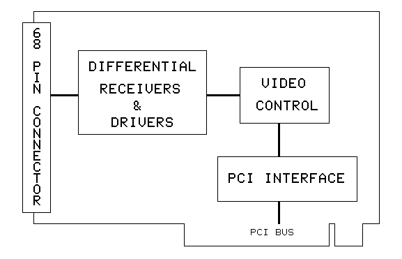
PIXCI D, PIXCI D24, & D2X Block Diagram
6.1. Differential Receivers and Drivers
The differential receivers and drivers convert data from differential to single ended TTL signals. Differential signals are used to provide improved noise performance over single ended TTL signals.6.2. Video Control
A field programmable gate array (FPGA) is used for image data formatting, video windowing, camera triggering, exposure timing, trigger conditioning, strobe generation, and buffering of data from the differential receivers to the PCI interface.6.3. PCI Interface
The PCI bus interface provides interrupt generation, PCI configuration registers, first-in and first-out buffers, and PCI bus master and target control.7. Specifications
7.1. Signal Input and Output:
The Dalsa CA-D6 and CT-P1 cameras use EIA RS-644 drivers and receivers.7.1.1. EIA RS-644 Low Voltage Differential Signaling Devices (LVDS)
-
National Semiconductor DS90C031TM driver.
Voltage Output Low Minimum: 0.9 Volts.
Voltage Output High Maximum: 1.6 Volts.
Absolute Maximum Output Voltage Range: -0.3 volts to VCC +0.3 volts. -
National Semiconductor DS90C032TM receiver.
Voltage Input Low Maximum: 0.8 Volts
Voltage Input High Minimum: 2.0 Volts
Absolute Maximum Input Voltage Range: -0.3 volts to VCC +0.3 volts.
7.1.2. Resolution:
Pixels: 8 to 4096 pixels per line. Pixel offset from horizontal drive: 0 to 8 pixels less than the number of pixel clocks per line from the camera.
Lines: 1 to 4096 lines per image. Line offset from vertical drive: 0 to 1 less than the maximum number of lines from the camera.
7.1.3. Frame Rate
The frame rate of the camera determines the frame rate of the PIXCI D32.
7.1.4. Bus Requirements
- 32 bit, PCI bus master, 33 MHz PCI slot, without shared interrupts.
- 1.55 Amps @ +5 Volts
- 4.913 inches long by 4.20 inches high (short slot).
7.1.5. Transfer Rates
Requires a burst mode PCI motherboard capable of sustained transfer rates to motherboard DRAM equal to or greater than the peak byte transfer rate of the camera. A motherboard with an AGP slot for the VGA adapter or AGP VGA on the motherboard is suggested. For a list of tested motherboards, see the ''Installation'' chapter or contact EPIX or an EPIX distributor for suggested motherboards.7.1.6. Display - DOS
- Any S/VGA with VESA support and a monochrome or color monitor. Display of false colored images requires VESA mode 112 support.
7.1.7. Display - Windows
- For XCAP: a 24 bit per pixel Windows compatible display system. Display resolution as per installed VGA device driver.
7.1.8. Connections
- 100 pin SCSI type connector. Honda part number PCS-XE100LFD-HS or equivalent used on board.
- Cables may be purchased separately.
Specifications subject to change without notice.
8. Camera Control Registers
The camera control registers generate the EXSYN and PRIN signals to the camera. Some cameras do not support PRIN. The camera control state machine can be used to trigger an image capture from the rising or falling edge of the asynchronous trigger input to the PIXCI D32. The camera control state machine can control the integration of the CA-D6 camera from minimum of 188 camera clocks at the maximum frame rate of 955 frames per second to 1.3 seconds at a frame rate of 0.7 frames per second using the 25 MHz camera pixel clock. The PRIN signal can be used to shorten the exposure time of the camera when the camera is running at maximum frame rate or when using the camera for triggered capture. The Dalsa CA-D6 camera used in test did not support PRIN.
A timing diagram showing trigger input, PRIN, EXSYN, and FVAL when using the camera for triggered capture is shown below. PRIN is held low until the trigger input is received. The EXSYN counter is used to provide exposure control of the camera. When the EXSYN counter reaches 0, EXSYN is generated to the camera to start readout of the image, which makes FVAL go high. After the image has been read out, FVAL goes low and a trigger can be accepted. Note that trigger inputs that take place between the time of the accepted trigger and the time that FVAL goes low will be rejected.
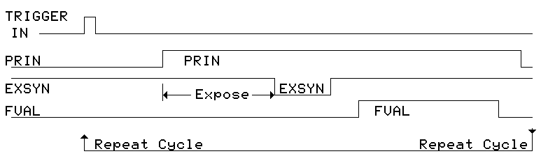
PIXCI D32 Dalsa Triggered Timing Diagram
A timing diagram showing PRIN, EXSYN, and FVAL when using the camera for electonic shuttering is shown below. The EXSYN counter is used to provide control the frame rate of the camera. When the EXSYN counter reaches 0, EXSYN is generated to the camera to start readout of the image, which makes FVAL go high. After FVAL goes high, the PRIN counter is loaded and starts counting down. PRIN goes low, dumping the charge stored on the sensor. When the PRIN counter reaches zero, PRIN goes high starting exposure of the sensor. Exposure continues until readout FVAL goes low, after the image has been read out.
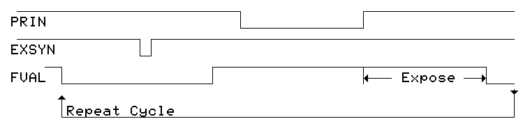
PIXCI D32 Dalsa Extended Integration Timing Diagram
A timing diagram showing PRIN, EXSYN, and FVAL when using the camera for extended integration is shown below. PRIN is held high (not used). The EXSYN counter is used to provide exposure control of the camera. When the EXSYN counter reaches 0, EXSYN is generated to the camera to start readout of the image, which makes FVAL go high. After the image has been read out, FVAL goes low and the EXSYN counter is loaded with the exposure count.
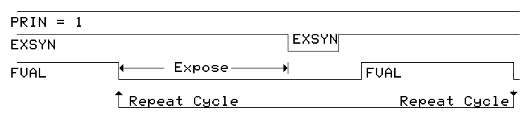
PIXCI D32 Dalsa Extended Integration Timing Diagram
8.1. XCLIB Trigger and Camera Integration Register Programming
The EXSYNC and PRIN 16 bit count values, which are the upper 16 bits of 32 bit registers, are programmed in the XCLIB ''C'' library with the following function:
int pxd_setExsyncPrin(unitmap, uint exsync, uint prin);
The lower 16 bit values of these registers are programmed by loading a video configuration format file previously saved by XCAP.
Refer to the XCLIB
''C''
Library User's Manual for additional programming information.
8.2. XCOBJ Trigger and Camera Integration Register Programming
The EXSYNC register and the PRIN registers are programmed in the XCOBJ ''C'' library with the following function:
int pxd_setHitachi01(ulong PRINC, ulong EXSYNC);
Refer to the XCOBJ
''C''
Library User's Manual for additional programming information.
0x0010 (PRINC). Pixel Reset INput Count. Write Only. 16 bits.
0x0000 on power up.
Bits 31 thru 16 control the duration of PRIN to the Dalsa camera.
16 bit down counter which is clocked by the camera clock output divided
by 4 thru by 512 (divide selected by bits 9 thru 7).
Bit 15, Vertical Drive Select.
Bit 15=1 PIXCI D32 generates vertical drive.
Note that the camera must be set for at least a 16 pixel clock delay after
rising edge of LEN when using a horizontal offset of less than 8.
Bit 15=0 PIXCI D32 accepts vertical drive from the 68 pin connector.
Bit 12, Line/Area Scan select.
Bit 12=1 waits for (LEN) HDIN =1 after the generation of EXSYNC.
Bit 12=0 waits for (FEN) VDIN =1 after the generation of EXSYNC.
Bit 11, MCK select.
Bit 11=1 selects the ICD2053B clock output to the camera.
Bit 11=0 selects a 1 for MCLK to the camera which causes the camera to use
the camera internal clock.
Bit 10, BIN select.
Bit 10=1 selects binning of pixels in the camera.
Binning is a camera option.
Binning decreases the resolution of the camera and increases light sensitivity.
Bit 10=0 selects no binning (power up default).
Bits 9 thru 7 control the camera clock divide selection for the state
machine clock.
Bits 9 thru 7 =111 select divide by 512.
Bits 9 thru 7 =110 select divide by 256.
Bits 9 thru 7 =101 select divide by 128.
Bits 9 thru 7 =100 select divide by 64.
Bits 9 thru 7 =011 select divide by 32.
Bits 9 thru 7 =010 select divide by 16.
Bits 9 thru 7 =001 select divide by 8.
Bits 9 thru 7 =000 select divide by 4.
Bit 6, not used.
Bit 5, STRS, Strobe Select.
Bit 5=1 selects a negative STRB output.
Bit 5=0 selects a positive STRB output.
Note that Strobe output is two camera control states later than PRIN.
Bit 4, TRIGNEG, Trigger Input Polarity Select.
Bit 4=1 selects a 1 to 0 transition of the Trigger input.
Bit 4=0 selects a 0 to 1 transition of the Trigger input.
The trigger input can be used to initiate the PRIN, EXSYNC
cycle.
Used for polarity selection for the trigger input.
Note that the trigger is also sent to the mailbox register.
Trigger input is clocked within 25 nanoseconds of the trigger edge.
The EXSYN to the camera is produced 3 camera control states later plus
the count for EXYNC.
Jitter between the trigger and EXSYN is a function of the camera clock
divider count used to provide a clock to the camera state machine.
Smaller numeric values for the camera clock divider will yield less jitter.
Bit 3, PRIN select.
Bit 3=1 selects output of PRINC counter to drive PRIN to camera.
On some cameras, PRIN is not available or is a camera option.
Bit 3=0 selects a one for PRIN (PRIN not used, power up default).
Bit 2, EXSYNC select.
Bit 2=1 selects the output of EXSYNC counter to drive EXSYN to camera,
if available (camera option).
Bit 2=0 selects a zero for EXSYNC (EXSYNC not used, power up default).
When EXSYNC=0, camera operates at maximum frame rate.
Bit 1, CNTS, Continuous Select.
Bit 1=1 selects continuous operation of the EXSYNC state machine.
Bit 1=0 selects single shot operation of EXSYNC.
Bit 0, TIS, Trigger Input Select.
Bit 0=1 causes the loading of the PRIN counter to be delayed until the trigger
input goes from 0 to 1.
Bit 0=0 ignores the trigger input and causes the
PRIN counter to be loaded after FVAL=1 (area) or LVAL (line) has been
received from the camera.
0x0014 (EC). External sync Count. Write Only. 16 bits.
0x0000 on power up.
Bits 31 thru 16 control the time between PRIN and EXSYNC.
16 bit down counter which is clocked by the state machine clock.
The sum of the time for PRINC, EC, and the time for the camera to generate
FVAL after EXSYNC is the frame period of the camera.
The count down time for PRINC is used regardless of the setting for
the PRIN select bit.
Writing this register when in the CNTS=0 will cause a single sequence of the
state machine to operate.
Notes on values used for CA-D6-0256W to achieve an EXSYN driven rate of 955
frames per second.
These values tested on one camera.
Value for External Sync Count may have to be increased on other cameras due
to variations in cameras.
Vdrive= Slaved
Line Scan Mode= VDIN=1
Clock to Camera= Internal
Pixel Binning= On
STRB Output= User selectable
Trigger Input Polarity= User selectable
PRIN= User Selectable
EXSYN= Driven by EXSYNC
EXSYN Operation= Continuous
PRIN Loaded= FVAL/LVAL
Camera Clock Divisor= 4 (minimum with the External Sync Count, below)
External Sync Count= 44 (minimum with the Camera Clock Divisor, above)
PRIN Duration= 200 (used for the ATI ring LED strobe)
Notes on values used for CA-D6-0256W to achieve an EXSYN driven rate of 0.74
frames per second, with an exposure of 1.342 seconds.
The sensor exhibits pixel gain variations that show up as white speckles.
The lens aperture is almost completely closed.
Settings as above with the following differences:
Camera Clock Divisor= 512.
External Sync Count= 65535.
9. In Case of Trouble
9.1. Software Problems - XCAP Error Messages
After XCAP is started and prior to the display of the first menu, the software checks for the presence of required BIOS software, the presence of the PIXCI D32 imaging board, and performs other tests. If any of the software checks fail, an error message will be displayed.
If error messages about ``FIFO Overflow'' are displayed, check the PC's setup
menu to see if PCI burst mode is enabled.
If burst mode is not enabled, the number of pixels per line may be limited
to 200 pixels or less.
Disable the clock in the taskbar on Windows 95 or NT.
Disable any other Windows applications that may periodically start.
Typing ``Ctrl-Alt Del'' in Windows will give a list of
applications that are running.
9.2. Hardware Problems
Some problems do not cause software error messages. Some problems may prevent the computer from powering up. Some problems may prevent the software from accessing the PIXCI D32 imaging board. These types of problems can be due to:| Power Supply | Insufficient power for the boards installed. |
|---|---|
| Touching Boards | One board's components are touching another board. |
| Defective Cable(s) | Camera cable has an open or short. |
| Video Input | Defective or incompatible video source. |
| Defective PIXCI D32 imaging board | Defective integrated circuit, bad solder joint, |
| physical damage, or static damage. | |
| Motherboard | No PCI burst mode or no PCI BIOS. |
| Defective PCI connector. | |
| PCI slot is not bus master capable. | |
| PCI slot shares interrupts or other resources with adjacent slot. | |
| S/VGA | S/VGA board is too slow, has insufficient memory, or is not a PCI board. |
9.2.1. Power Supply Problems
The PC power supply usually has a printed rating of power available for the four standard PC voltages. The PIXCI D32 imaging board uses 1.4 amps from the +5 volt supply. If other devices and the PIXCI D32 imaging board use more power than the power supply can provide, the power supply will shut down. In marginal situations, this may not happen until an operation is performed that requires additional power, such as increasing the number of pixels per line. Try removing non-essential boards from the system.9.2.2. Touching Boards
If the components of one board touch those of another, damage to one or both boards can occur. Move one of the touching boards at least one slot away from the other.9.2.3. Defective Cable
If the camera cable is broken or shorted, the board may not function or may intermittently function.- Try another cable.
- Test the cable for shorts or opens with an ohmmeter.
9.2.4. Camera Input
If the camera is defective, has the lens closed or covered, or has the exposure set for a time that is too short for the amount of light available, a black image will be captured.- Select the ``Modify'' menu and select ``Patterns.'' Write a test pattern to image memory which will be displayed on the monitor. Snap an image to see if the test pattern is written over by the camera's video data. If the test pattern is not overwritten, the camera, camera cable, or camera power supply may be defective.
- If the test pattern is overwritten, the camera lens may be closed, the cap may be covering the lens, or the exposure may be too short.
9.2.5. Motherboard
- If the motherboard does not support PCI burst mode, does not have a PCI BIOS, or the PIXCI D32 imaging board does not operate correctly, try another motherboard. Call EPIX for a list of suggested motherboards.
- The PCI bus connector on the motherboard may be defective. Try another PCI bus slot or another motherboard.
- The PCI bus slot may not support a PCI master. Try another PCI bus slot or another motherboard.
- The PCI bus slot may be wired to share interrupts or other slot resources with one of the adjacent slots. Try another PCI bus slot or another motherboard.
9.2.6. S/VGA Board
If the S/VGA board has insufficient memory, is not a PCI board, does not support PCI burst mode, or the XCAP software does not operate correctly, try another S/VGA board. Call EPIX for a list of suggested S/VGA boards.9.3. If All Else Fails
If none of the above suggestions have solved the problem, call your distributor (if you purchased the board thru a distributor), or FAX or e-mail EPIX for technical support. In the FAX or e-mail, include error messages that were displayed, describe symptoms observed, and steps taken to attempt to solve the problem. It is helpful to call from a phone near the computer with the PIXCI D32 imaging board installed.The PIXCI D32 imaging board can be damaged during shipment. If damage is visible, check the shipping container for damage, and notify the freight carrier.
If the board must be returned for test or repair, call EPIX for a Return
Materials Authorization (RMA) number.
Be prepared to describe
the problem that has been encountered and what steps have been taken
to attempt to correct it.
Please include a written description of symptoms, error messages, and
steps taken to attempt to solve the problem with
the packing list for the material returned.
9.4. Receiver Outputs
At location B1, the DS90C032 differential receiver has outputs: pixel clock, pin 13, LEN (horizontal drive, pin 3), and FEN (vertical drive, pin 11).
The pixel clock is used to clock camera data on the rising edge. Horizontal and vertical drive are used to accept camera data when high.
10. Hardware Revision Description
10.1. PIXCI D32
-
Revision 0.0:
Released without changes.
-
Revision 1.0:
Moved 100 pin connector in 0.04 inches. Very tight fit against chassis. Layout error correction.
Removed +5 volts and +12 volts from header pins 2 and 4.
Added TTL EXE (EXSYN), and TTL EXS (STRB) to header pins 2 and 4.
- Corrected swap of video data bits 0&1, 4&5, and 12&13 which had been performed in the FPGA on Revision 0.0.
11. Certification and Warranty
11.1. Certification and Testing
The PIXCI D32 imaging board has been tested per EMC directive 89/336/EEC and has met the following test requirements:
- EN 50081-1/01.92,
- EN 55022/08.94 class B
- EN 61000-4-2/03.95
- ENV 50204/03.95
These test are more commonly known as the ``CE'' test. The testing was performed to class B which has a more restrictive emission limit than the FCC class B limit.
If you find that the computer system in which the PIXCI D32 is installed is causing interference with other devices, try increasing the distance between the devices, reorienting (turning) the devices, or using additional shielding on the computer system (such as placing covers on the computer and installing metal shields in unused slots or over unused drive slots).
It may be that the camera connected to the PIXCI D32 is the source of radiation.
To determine if the camera is the source of interference, remove power to the
camera.
If a shielded camera cable is not being used, use a shielded cable.
If the camera is the source of interference, contact the camera manufacturer.
11.2. Limited Warranty
EPIX, Inc. warrants to the original purchaser of the PIXCI D32 board that
the PIXCI D32 board shall be in good working order for
a period of one year from the date of shipment from EPIX, Inc.
Should this product fail to be in good working order at any time during
this one year warranty period, EPIX, Inc.
will, at its option, repair or replace this product at no additional
charge except as set forth below.
Repair parts and replacement
products will be furnished on an exchange basis and will be either
reconditioned or new.
All replaced parts and products become the property of EPIX, Inc.
This limited warranty does not include service to
repair damage to the product resulting from accident, disaster,
misuse, abuse, or non-EPIX, Inc. modification of the product.
Limited warranty service may be obtained by delivering the product
during the one year warranty period to an EPIX, Inc. distributor or
to EPIX, Inc. and providing proof of the purchase date.
Insure the product or assume the risk of loss or damage in transit.
Prepay shipping charges to EPIX, Inc. or to the distributor.
Use the original shipping container, or the equivalent,
and static dissipative packaging material.
EPIX, Inc. hereby disclaims all other express and implied warranties for
this product, including the warranties of merchantability and fitness
for a particular purpose.
Some states do not allow the exclusion of
implied warranties, so the above limitations may not apply to you.
If this product is not in good working order as warranted above, your
sole remedy shall be repair or replacement as provided above.
In no event will EPIX, Inc. be liable to you for any damages, including any lost
profits, lost savings or other incidental or consequential damages
arising out of the use of or inability to use such product, even if
EPIX, Inc. or an authorized EPIX, Inc. distributor has been advised of the possibility
of such damages, or for any claim by any other party.
12. Footnotes
- [1]
- If modifying a previously installed XCAP: Right click the XCAP icon, select ''Properties'', select ''Program'', and modify the ''Name'' or ''Command Line'' as needed.
- [2]
- If the PC is configured with a selective boot option (i.e. so as to boot Windows or boot old DOS), be sure to modify the correct CONFIG.SYS.
- [3]
- If modifying a previously installed XCAP: Right click the XCAP icon, select ''Properties'', select ''Program'', and modify the ''Name'' or ''Command Line'' as needed.
- [4]
- If modifying a previously installed XCAP: Right click the XCAP icon, select ''Properties'', select ''Program'', and modify the ''Name'' or ''Command Line'' as needed.
- [5]
- The identification code is provided on a card enclosed with the CD or diskette(s), and is also shown on the packing list. The card and the identification code may be required as proof of purchase for future software upgrades. Keep the card in a safe place!!
- [6]
- XCAP-Std and XCAP-Plus also require an authorization key to activate all features.
- [7]
- The required ''XCAP Sourcery'' TWAIN driver is a separate software product and is not included with XCAP.
- [8]
- The required ''XCAP Sourcery'' Image-Pro driver is a separate software product and is not included with XCAP.